What is the investment cost for large-area OLED that will lead the premium TV market?

■ Investment cost comparison and analysis for WRGB OLED, solution processed OLED and QD-OLED
■ Total OLED process equipment is expected to form a market of US$ 58.8 billion from 2018 to 2022, and inspection equipment market is estimated as US$ 8.4 billion

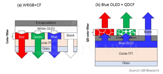
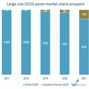
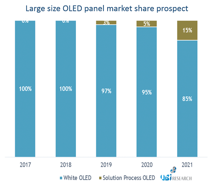
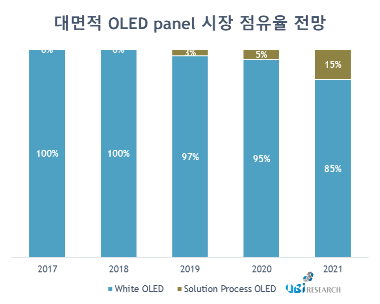
In the premium TV market, the market share of OLED TVs is steadily rising, and the number of OLED TV camps is gradually increasing. OLED TV adopts color filter to WRGB OLED, and currently LG Display only mass produces the OLED panels.

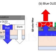
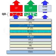
On the other hand, Samsung Display is developing QD-OLED (blue OLED + quantum dot color filter) to compete with WRGB OLED in the premium TV market. Blue OLED is a technology in which the blue light emitted from OLED passes through a quantum dot layer and a color filter to represent red and green colors.

<Expected structure of QD-OLED>

UBI Research analyzed the structure and investment amount of WRGB OLED and QD-OLED, which are the latest issues, in the‘AMOLED Manufacturing and Inspection Equipment Industry Report’ published on June 6. In addition, the investment amount of the solution process OLED, which has got the industry attention due to its possible implementation of real RGB in large-area OLED, is also analyzed and compared.

As a result of analyzing the equipment investment cost based on the 8th generation 26K, the QD-OLED investment cost is 3% higher than WRGB OLED and the investment cost of solution process OLED is 19% less than that of WRGB OLED.

In the QD-OLED investment cost, it is reflected that QD color filter is separately formed and its laminating process is added. For the analysis of solution processed OLED investment cost, color filter is excluded and ink-jet printer is applied instead of deposition equipment.

In addition, the report forecasts the overall OLED equipment market from 2018 to 2022. The total OLED overall equipment market is expected to reach US$ 106.7 billion from 2018 to 2022. The market for process equipment is projected as US$ 58.8 billion and inspection equipment market is to be US$ 8.4 billion.

Premium TV 시장을 주도할 대면적 OLED의 투자 비용은?

최근 premium TV 시장은 OLED TV의 점유율이 지속적으로 상승하고 있으며 OLED TV 진영도 꾸준히 증가하고 있는 추세다. OLED TV는 WRGB OLED에 color filter를 적용한 구조로써, 현재 LG Display만이 유일하게 OLED panel을 양산하고 있다.

이에 Samsung Display에서는 premium TV 시장에서 WRGB OLED에 대항하기 위해 blue OLED + quantum dot color filter(이하 QD-OLED)를 개발하고 있는 것으로 알려졌다. Blue OLED는 OLED에서 발광 된 청색광이 quantum dot층과 color filter를 통과해 red와 green 색을 나타내는 기술이다.

<QD-OLED 예상 구조>

유비리서치는 지난 6일 발간한 ‘AMOLED Manufacturing and Inspection Equipment Industry Report’에서 최근 이슈가 되고 있는 WRGB OLED와 QD-OLED의 구조와 투자 금액을 분석했다. 뿐만 아니라, 대면적 OLED에서 real RGB를 구현할 수 있어 주목받고 있는 solution process OLED의 투자 금액도 함께 분석하여 비교했다.

8세대 26K 기준으로 장비 신규 투자비를 분석한 결과, QD-OLED 투자비는 WRGB OLED에 비해 3%가 많고 solution process OLED는 WRGB OLED에 비해 19% 적은 것으로 조사되었다.

QD-OLED 투자비에서는 QD color filter가 따로 형성되고 이를 합착하는 공정이 추가된 내용이 반영되었으며, solution process OLED 투자비에서는 color filter가 제거되고 증착 장비 대신 ink-jet printer가 투입된 내용이 반영되었다.

이 밖에 본 보고서에서는 2018년부터 2022년까지 OLED 전체 장비 시장도 예상하였다. 2018년부터 2022년까지 OLED 전체 장비 시장은 US$ 106.7 billion을 형성할 것으로 전망되며, 공정 장비는 그 중 US$ 58.8 billion, 검사 장비는 US$ 8.4 billion의 시장을 형성할 것으로 예상된다.

<2018년~2022년 장비별 전체 시장 점유율 전망>

가상현실 주도하는 OLED 초고해상도 경쟁 시작됐다.

최근 VR 기기 set 업체들과 OLED panel 업체들이 mobile 기기보다 뛰어난 해상도의 OLED가 적용 된 VR 기기와 VR 기기용으로 제작 된 초고해상도 OLED를 선보이며 이목을 집중시키고 있다.

지난 CES 2018에서 공개 된 VIVE PRO가 최근 신제품 발표회를 통해 국내에 공식 런칭되었다. VIVE PRO는 전작인 HTC VIVE의 448ppi 보다 78% 향상 된 615ppi 해상도의 OLED가 탑재되었다.

<HTC VIVE Pro, Source: vive.com>

뿐만 아니라 최근 OLED panel 업체들도 VR 기기용 초고해상도 OLED를 다수 선보이고 있다. 지난 SID 2018에서 LG Display는 Google과 공동 개발한 1443ppi VR기기용 OLED를 공개했다. 기존의 OLED는 538ppi 수준이었으나 LG Display는 WRGB + CF 방식을 적용하여 UHD(3840 x 4800) 해상도를 구현했다.

<SID 2018에서 공개 된 LG Display의 1443ppi OLED>

Samsung Display도 SID 2018에서 1,200 ppi 해상도의 2.43 inch OLED panel 2개로 제작된 VR 기기를 전시하였다. RGB OLED가 적용 된 이 VR기기는 전년도 858ppi 보다 해상도가 더욱 더 향상 된 OLED가 적용되었다.

Sony도 지난 5월 4,032ppi의 VR 기기용 micro OLED인 ‘ECX339A’의 상용화를 발표하였다. 크기는 0.5 inch로 240fps까지의 프레임 속도 지원도 가능한 것으로 알려졌다. 양산시기는 2018년 11월이다.

VR 기기는 눈과 디스플레이 사이의 거리가 매우 짧기 때문에, 해상도가 낮으면 디스플레이의 픽셀 무늬들이 격자 형태로 보이는 ‘모기장(Side door effect)’ 현상이 나타난다. 이로 인해 눈의 피로를 가중시키며 현실성을 떨어뜨리기 때문에 panel 업체에서는 고해상도 OLED 개발에 집중하고 있으며 Sony나 Facebook(Oculus VR) 같은 set 업체에서도 고해상도 OLED를 VR 기기에 적용하고 있다.

최근 들어 Set 업체 뿐만 아니라 OLED panel 업체들도 다양한 방식으로 기존보다 더욱 더 업그레이드 된 고해상도의 OLED와 VR기기를 다수 선보이고 있어 향후 더욱 더 높은 해상도의 VR용 기기가 상용화 될 수 있을지 귀추가 주목된다.

The competition for ultra-high resolution of OLED that led virtual reality was started.

Recently, set makers are introducing VR devices with higher resolution OLED than mobile devices, and OLED panel makers are focusing attention on developing ultra-high-resolution OLEDs designed for VR devices.

VIVE PRO, which was unveiled at CES 2018, was officially launched in Korea through a new product presentation. VIVE PRO is equipped with 3K resolution and 615ppi OLED, which are upgraded 78% from 448ppi of the previous HTC VIVE.

<HTC VIVE Pro, Source: vive.com>

In addition, OLED panel makers has introduced a number of ultra-high-resolution OLEDs for VR devices. In SID 2018, LG Display unveiled an OLED for 1443ppi VR device, jointly developed with Google. The resolution of conventional OLEDs was at 538ppi level, but LG Display accomplished UHD (3840 x 4800) resolution by applying WRGB + CF.

<LG Display’s 1443ppi OLED, introduced in SID 2018>

Samsung Display also exhibited VR devices made with two 2.43-inch OLED panels at 1,200ppi resolution in SID 2018. The resolution of this VR device, applied with RGB OLED, is much higher than the previous year’s 858ppi.

Sony also announced the commercialization of ‘ECX339A’, a micro OLED for 4,032ppi VR devices, in May. It is also possible to support a frame rate of up to 240fps at 0.5 inches in size. The mass production schedule is November 2018.

Since the distance between the eyes and the display is very short, a VR device shows a ‘side door effect’ in which the pixel patterns of the display are displayed in a lattice form when the resolution is low. As this problem increases eye fatigue and diminishes the reality, panel makers are focusing on high-resolution OLED development, and set makers such as Sony and Facebook (Oculus VR) are applying high-resolution OLEDs to the VR devices.

Recently, not only set makers but also OLED panel makers have introduced a number of high-resolution OLED and VR devices, which have been upgraded more than ever before. Attention is growing whether higher resolution VR devices will be commercialized in the future.

Sony, UXGA 해상도의 0.5 inch micro OLED 상용화 발표

Sony는 UXGA 해상도의 0.5 inch OLED micro display인 ‘ECX339A’의 상용화를 발표하였다. Sony는이 제품이 세계에서 가장 작은 6.3 um 픽셀 피치(pixel pitch)를 달성하여 이전 제품인 ECX337A”(0.5 인치 QVGA (1280 × 960) 대비 1.6배의 고해상도 구현에 성공하였다고 밝혔다.

<Sony의 0.5 inch micro OLED ‘ECX339A’, Source: sony.co.jp>

또한, 기존 대비 50% 전압에서 동작하는 새로운 구동 회로가 적용되어 저전력 구동과 함께 dual-line progressive 구동 방식을 통해 240fps까지의 프레임 속도 지원도 가능하다고 언급했다.

<신 제품(좌)과 기존 제품(우) micro OLED 해상도 비교, Source: sony.co.jp>

Sony에 따르면, 기존의 micro display의 고해상도화는 픽셀 피치 축소에 따른 화질 저하와 시야각 특성 악화 등의 문제가 있었으나 Sony의 트랜지스터 레이아웃과 프로세스의 최적화, 보정 회로 적용을 통해 이를 개선하였다고 밝혔다. 또한, color filter를 직접 실리콘 기판에 형성하여 발광층과의 거리를 줄이고, color filter의 색 배치를 고안하여 시야각 특성을 향상하고 고해상도를 실현하였다고 설명했다.

<신 제품(좌)과 기존 제품(우)의 구조와 시야각 특성 이미지, Source: sony.co.jp>

ECX339A의 예정 양산시기는 2018년 11월이며 샘플 가격은 50,000엔(세금 별도)로 책정 되었다. Sony는 이번 제품이 화질 요구가 가장 많은 하이엔드 카메라와 가상현실용 HMD(head mounted display)에 적용 될 것으로 예상했다.

<ECX339A 주요 사양, Source: sony.co.jp>

Sony, announced the commercialization of 0.5-inch micro OLED with UXGA resolution

Sony announced the upcoming release of the ‘ECX339A’, a 0.5-inch OLED micro-display with UXGA resolution. According to Sony, it has achieved the world’s smallest pixel pitch of 6.3 μm, enabling a resolution 1.6 times higher than its predecessor, “ECX337A “(0.5-inch QVGA (1280 × 960)).

<Sony’s 0.5 inch micro OLED ‘ECX339A’, Source: sony.co.jp>

By employing newly-designed peripheral circuits that operate on half the voltage of previous model, it supports a high frame rate of up to 240 fps, with dual line progressive driving technique and low power operation.

<Comparison of OLED resolution between new product(left) and previous product(right), Source: sony.co.jp>

According to Sony, the high resolution of the existing micro display had problems such as deterioration in picture quality and deterioration in viewing angle due to pixel pitch reduction; however, they have been improved by Sony’s transistor layout, process optimization, and compensation circuit. In addition, the color filter is deposited directly on the silicon substrate, reducing its distance from the light emitting layer, and the filter’s color array has been modified to secure the viewing angle properties while achieving high resolution.

<Structure and viewing angle image, new product (left) and previous product (right), Source: sony.co.jp>

The mass production schedule for the ECX339A is November 2018, and the sample price is set at JPY 50,000 (Tax not included). Sony expects this product to be applied to high-end cameras and head-mounted displays for virtual reality, which require the highest picture quality.

<ECX339A, key specifications, Source: sony.co.jp>


Can BLUE OLED be used for OLED TV?

Samsung Display selected blue OLED + QDCF (blue OLED) as next generation display technology following LCD TV, and started the necessary development.

Blue OLED is a technology, in which blue light emitted from blue OLED passes through a quantum dot color filter to represent red and green colors (b). The WRGB OLED used in OLED TV is a method in which white light passes through a color filter and implements RGB colors (a).

The ‘2018 OLED Materials Industry Report’ published by UBI Research on April 18 describes whether blue OLED, which Samsung Display has started to develop, can become TV OLED panels. The expected development direction and performance (efficiency and lifetime) of blue OLED + QDCF are analyzed. In particular, current status and development trends (fluorescence, phosphorescence, TADF) of blue emitting material, which is the core material of blue OLED, are covered.

Since blue OLED of Samsung Display is top emission type, the aperture ratio is increased by about 70% compared to the bottom emission, which emits light in the TFT direction, so that 8K resolution and high brightness are realized better than the conventional WRGB OLED. In addition, it is expected to reach BT. 2020, the UHD color standard, which was established by the International Telecommunication Union (ITU) in 2012, using QD material with high color reproduction rate as color filter.

In the future premium TV market, 8K and BT. 2020 are necessary conditions for display. WRGB OLED is also being actively developed to implement 8K and BT2020. Attention is focused on the impact of the development of blue OLED in the premium TV market led by WRGB OLED.

In addition, the report analyzes the market status and development trends of the related companies, including overall technology development directions and key issues for new materials such as soluble OLED materials and near IR materials.

BLUE OLED가 OLED TV에 사용될 수 있을까?

삼성디스플레이가 LCD TV를 이을 차세대 디스플레이 기술로서 blue OLED + QDCF(이하 blue OLED)를 선정하고 개발에 착수 했다.

Blue OLED는 OLED에서 발광 된 청색광이 quantum dot층과 color filter를 통과해 red와 green 색을 나타내는 기술이다(b). OLED TV에 사용중인 WRGB OLED는 백색광이 칼라필터를 통과해 RGB 색상을 구현하는 방식이다(a).

유비리서치가 지난 18일 발간한 ‘2018 OLED 발광재료 산업 보고서’는 삼성디스플레이가 개발에 착수한 blue OLED가 TV용 OLED 패널이 될 수 있는지를 분석하였다. blue OLED+QDCF의 예상 개발 방향과 기대되는 성능(효율과 수명)을 분석하였으며, 특히 blue OLED의 핵심 재료인 blue 발광재료의 현재 동향과 개발 상황(형광, 인광, TADF)을 다루고 있다.

삼성디스플레이의 blue OLED는 top emission 방식이기 때문에 TFT 방향으로 빛이 방출되는 bottom emission 대비 개구율이 약 70% 증가되어 8K 해상도와 고휘도 구현이 기존 WRGB OLED보다 유리하다. 또한, 색재현율이 높은 QD 재료를 color filter로 사용하여 2012년 국제 전기 통신 연합인 International Telecommunication Union(ITU)가 제정한 UHD 색 규격인 BT. 2020에 도달이 가능할 것으로 예상된다.

추후 프리미엄 TV 시장에서 8K와 BT2020은 display가 갖추어야할 필수조건으로 WRGB OLED도 8K와 BT2020을 구현하기 위해 적극적으로 개발 중에 있다. Blue OLED의 개발이 WRGB OLED가 주도하고 있는 프리미엄 TV시장에서 앞으로 어떤 영향을 미칠지 기대된다.

그 밖에도 soluble OLED 재료와 near IR 재료 등 신규 재료들에 대한 전반적인 기술 개발 동향과 핵심 이슈를 다루었다.

유비리서치 OLED 최신기술 동향 세미나 개최

  • 최근 폴더블OLED와 solution processed OLED, 대면적 blue OLED, Micro LED, 양자점(Quantum Dots)등 가장 이슈가 되고 있는 차세대 디스플레이 관련 기술 및 전망 발표
  • 다양한 디스플레이 소재 기술에 관한 연구 및 주요 기술 동향 발표

유비산업리서치(http://www.ubiresearch.co.kr/, 대표 이충훈)는 오는 4월 26일(목) 서울 코엑스 전시장 3층 Hall E에서 ‘OLED 최신기술 동향 세미나’를 개최 할 예정이다.

CES2018에서 삼성디스플레이는 blue OLED에 quantum dot와 color filter를 사용한 새로운 구조의 OLED 패널을 공개했다. 이 구조의 OLED는 삼성디스플레이의 현재 사업인 모바일용 디스플레이가 아닌 TV용 대면적 OLED제작을 위한 패널이다.

삼성디스플레이가 blue-OLED 개발에 착수하기 위해 대규모 개발팀을 신설한 것은 LG디스플레이가 독보적으로 차지하고 있는 대면적 OLED 패널 사업에 진입하기 위한 사전 포석 단계로 볼 수 있다. 이번 세미나에서는 삼성디스플레이가 최근 공개한 계획인 blue-OLED의 사업화 가능성과 LG 디스플레이의 WRGB OLED와 비교하여 어떤 기술인지를 집중적으로 분석해 보고자 한다. 이를 위해 가장 중요한 해결 과제인blue OLED용 청색 발광 재료 개발 현황과 blue OLED용 quantum dot 재료 개발 현황을 면밀히 분석하여 전망할 예정이다.

또한 대면적 OLED 패널 이슈와 함께 모바일에서 새로운 Application에 대한 가능성으로 제시되고 있는 폴더블OLED개발 현황과 시장을 전망한다. 이를 통해 올초 계획인 2018년 연말 폴더블 OLED 스마트폰 출시와 관련한 다양한 예상이 가능할 것으로 기대한다.

그 이외에 또 다른 대면적 디스플레이 기술로서 이슈화되고 있는 solution processed OLED와 Micro LED등 차세대 디스플레이 기술 현황과 개발 이슈 사항 등을 다룰 예정이다.

이번 세미나는 빠르게 진화하는 디스플레이 시장의 기술 트랜드를 예측하여 업체들의 시장현황과 기술 변화를 파악하는데 큰 도움이 될 것으로 기대하고 있다.

금번 세미나의 세부 주제들로는 △’ OLED 스마트폰과 폴더블 폰 시장 전망’ △’OLED TV 프리미엄 시장 확대를 위한 핵심 기술 과제 – Solution Process OLED 가능성’ △ ‘폴딩 1R 구현을 위한 핵심기술 과제 – TFT, 기판, 인캡등’ △’BLUE OLED + QDCF TV 를 위한 핵심 기술 과제 : QD재료’ △’OLED TV용 Oxide TFT’ △ ‘OLED 청색 발광 재료 기술 동향 및 전망’ △ ‘Micro LED 프리미엄 TV 제조공정을 위한 핵심 기술 과제 등의 주제 발표가 예정되어 있다.

Developing ultra-definition display with a color filter technology

A color filter technology has been developed that can bring forward commercialization of next generation’s TVs with ultra-definition visibility and lower prices. The National Research Foundation of Korea (a chairman of the board, Moo-jae, Cho) announced that Prof. for Korea University, Byeong-kwon, Joo’s research team has developed a complementary plasmon color filter having sharp display and high resolution. The color filters which are currently used in the display industry mainly are optical absorption type using pigments or dyes. It has low chemical stability since it is based on organic materials and high unit cost due to manufacturing RGB filters separately. On the other hand, the optical interference type plasmon color filter using inorganic materials can simultaneously produce various color filters at low cost, but there is a problem that the color purity is in decline due to color interference occurring in the two-dimension array of nanostructures.

<Transmittance spectrum according to opening ratio of Hole pattern and dot pattern structures, Source: The National Research Foundation of Korea>

The research team applied a reversal approach to break out the existing pattern as complementary design method that combines dot pattern with hole pattern. It is a general viewpoint of academia that it is difficult to apply dot pattern to a transmission color filter in the form of reversing the existing hole pattern. However, the team assured that the extraction of high purity for red is possible through effective blocking the leakage of short wavelengths by dot pattern under certain conditions. The result is shown that the range of implementing color in the complementary designed plasmon color filter is widened over 30% than before.

<Plasmonic color filter of Hole pattern and Dot pattern structure produced, Source: The National Research Foundation of Korea>

In addition, the implementing of various color of the complementary plasmon color filters is available such as red, green, and blue by adjusting only the geometric parameters of the nanopattern. The performance can be improved without additional costs since the existing materials and manufacturing methods could be used as usual.

Prof. Byeong-kwon, Joo explained that “This research has developed a plasmon color filter with high color reproducibility through a complementary design method. This is expected to accelerate the development of the next-generation display combining nano-optic devices.”

The research results were performed by supporting of the Basic Research Support Project(private research) of the National Research Foundation of Korea at the Ministry of Science, ICT and Future Planning, the Ministry of Education·BK21 support project of the National Research Foundation. It was published in the Scientific Reports affiliated journal of an international journal Nature, on January, 13th.

초고화질 디스플레이 컬러필터 기술 개발

초고화질 선명도를 가지면서도 가격은 더욱 저렴한 차세대 TV 상용화를 앞당길 수 있는 컬러필터 기술이 개발되었다. 한국연구재단(이사장 조무제)은 주병권 교수(고려대) 연구팀이 선명하고 해상도가 높은 색을 나타낼 수 있는 상보형 플라즈몬 컬러 필터를 개발했다고 밝혔다. 현재 디스플레이 산업에서 주로 사용하는 컬러필터는 안료나 염료를 이용한 광흡수 방식이다. 이는 유기재료를 기반으로 하기 때문에 화학적 안정성이 낮고, RGB 필터를 각각 제조해야 하기 때문에 단가가 높다. 반면 무기재료를 사용하는 광간섭 방식의 플라즈몬 컬러필터는 저렴한 비용으로 다양한 색의 필터를 동시에 제조할 수는 있으나, 나노 구조물의 이차원 배열에서 발생하는 색의 간섭 현상 때문에 색 순도가 저하되는 문제점이 있다.

<Hole(음각) 패턴과 dot(양각) 패턴 구조의 개구 비율에 따른 투과 스펙트럼, 출처 : 한국연구재단>

연구팀은 음각 패턴에 양각 패턴을 조합하는 상보형 설계방법으로 기존의 정형화된 패턴 모양을 탈피하는 역발상을 적용했다. 양각 패턴은 기존의 음각 패턴을 반전시킨 형상으로 투과형 컬러필터에 응용하기 어렵다는 것이 학계의 일반적인 시각이었다. 그러나 연구팀은 특정 조건에서 양각패턴이 단파장의 누설을 효과적으로 차단함으로써 순도 높은 적색 추출이 가능함을 확인했다. 그 결과, 상보형으로 설계된 플라즈몬 컬러필터에서 색을 구현하는 영역이 이전보다 30% 이상 넓어지는 결과를 확인할 수 있었다.


<제작된 Hole(음각) 패턴과 dot(양각) 패턴 구조의 플라즈모닉 컬러필터, 출처 : 한국연구재단>


또한 상보형 플라즈몬 컬러필터는 나노 패턴의 기하학적 변수만 조절하면 적색, 녹색, 청색 등 다양한 색상 구현이 가능하다. 기존의 재료와 제조 방법을 그대로 사용할 수 있기 때문에 추가적인 비용 발생 없이 성능을 향상시킬 수 있다.


주병권 교수는“이 연구는 상보형 설계 방법을 통해 높은 색재현성의 플라즈몬 컬러필터를 개발한 것이다. 이 연구가 나노광학소자를 결합시킨 차세대 디스플레이의 개발을 앞당기는 계기가 될 것으로 기대된다.”라고 연구의 의의를 설명했다.


이 연구성과는 미래창조과학부 한국연구재단의 기초연구지원사업(개인연구), 교육부·한국연구재단의 BK21지원사업 등의 지원을 받아 수행되었다. 국제적인 학술지 네이처(Nature) 자매지인 사이언티픽 리포트(Scientific Reports) 1월 13일자에 게재되었다.


Solution Process OLED TV is prospected to be launched on the market in 2019, targeting the Mid-end TV Market

According to “Market Entry Analysis for Solution Process OLED -The Possibilities and Opportunities” issued on November 14 by Ubiresearch, OLED TV, produced in solution process method, is prospected to be launched on the market in 2019.

Solution process is a technology which enables producing OLED panel in RGB pixel structure without any panel division on a device higher than G8, which major AMOLED panel producers has actively engaged in developing.

However, lamp efficiency and life cycle have no option to decrease because luminescent materials have lower purity than that of evaporation materials as luminescent materials applied to solution process should be mixed with various solvents in order to make the existing evaporation materials ink. Nevertheless, why major panel producers has actively engaged in developing solution process is that production cost can be declined as the usage efficiency of luminescent materials is high without using color filters and its structure is simpler than that of OLED panel using WRGB method.

According to the report, it is said that although developing luminescent materials for solution process OLED has been fully engaged, it should be more efficient than that of WRGB methods so as to enter the premium market. However, it seems substantially difficult that the capacity of solution process OLED surpasses that of WRGB as WRGB has been developed in top emission structure to improve its efficiency by over 20% and evaporation materials have also constantly been developed. Rather, based on proper level of life cycle and efficiency, it would be competitive to replace LCD targeting the mid-end TV market, according to the report.

Issues on OLED, QLED, hybrid QD, which can be applied to solution process and possibilities to enter the market, comparative analysis on the capacity of present solution process OLED, supply chain of QD industries, and major soluble OLED material producers are included in this “Market Entry Analysis for Solution Process OLED -The Possibilities and Opportunities” and it is expected to help the relevant producers understand the solution process industry.

Meanwhile, it is predicted that the market of large-scaled solution process OLED panel over 55 inch will begin in earnest being mass-produced as of 2019 and have accounted for the entire wide OLED panel market by approximately 15% growing by approximately US$ 1,000 million by 2021.

Solution Process OLED TV 2019년 시장 출시 전망, Mid-end TV 시장 공략

유비산업리서치에서 11 14일 발간한 “Solution Process OLED 시장 진입가능성 분석 보고서”에 따르면 solution process로 제작된 OLED TV 2019년에 시장에 출시될 것으로 내다봤다.

Solution process는 대면적 OLED panel Gen8 이상의 장비에서 원장 분할 없이 RGB pixel 구조로 제조할 수 있는 기술이며 주요 AMOLED panel 업체에서 적극적으로 개발을 진행 중에 있다.

하지만 solution process에 적용되는 발광재료는 기존 증착재료를 ink화 시키기 위해 다양한solvent를 섞기 때문에 증착재료보다 순도가 낮아 발광효율이 떨어지고 수명이 낮을 수 밖에 없다. 그럼에도 불구하고 solution process를 주요 panel 업체들에서 적극적으로 개발하고 있는 이유는 color filter를 사용하지 않고 발광재료 사용효율이 높으며 WRGB방식의 OLED panel에 비해 구조가 단순하기 때문에 원가절감을 할 수 있다는 점이다.

보고서에 따르면 “Solution process OLED용 발광재료 개발이 적극적으로 이루어지고 있지만 프리미엄 시장에 진입하기 위해서는 WRGB 방식보다 효율이 좋아야 한다. 하지만 WRGB는 효율을 20%이상 높일 수 있는 top emission 구조로 개발 중이며 증착재료도 지속적으로 개발이 되고 있어 solution process OLED WRGB의 성능을 넘어서기는 상당히 어려울 것으로 예상된다. 오히려 적당한 수준의 수명과 효율을 바탕으로 mid-end TV 시장을 공략해 LCD를 대체하는 시나리오가 가장 유력할 것.” 으로 내다봤다.

이번에 발간된 Solution Process OLED 시장 진입가능성 분석 보고서에서는 solution process가 적용될 수 있는 OLED QLED, hybrid QD들의 이슈와 시장진입 가능성, 현재 solution process OLED QD 산업의 supply chain, 주요 soluble OLED material 업체들의 성능 비교 분석등을 수록하여 업체들에서 solution process 산업을 파악하는데 도움이 될 것으로 예상된다.

한편 Solution Process OLED 시장 진입가능성 분석 보고서 55inch 이상의 대면적 solution process OLED panel 시장은 2019년부터 본격적으로 양산되기 시작하여 2021년 약 US$ 1,000 million 규모로 성장하여 전체 대면적 OLED panel 시장의 약 15를 차지할 것으로 내다봤다.

161114_2


Aggressive investment on QLED, Shortcut of OLED commercialization

At ‘an analytical seminar on market entry potential of OLED and Solution Process OLED’ having been held in Seoul Small& Medium Business Center on last October 14th, Professor Lee Chang-hee of Seoul National University and Senior Researcher Bang Ji-won of Korea Institute of Ceramic Engineering and Technology shared opinions about current situations of QLED, development trends, and issues.

1610193

<Professor Lee Chang-hee of Seoul National University>

1610194

<Senior Researcher Bang Ji-won of Korea Institute of Ceramic Engineering and Technology>

Professor Lee Chang-hee said that QLED had excellent color purity because half-width of QLED was narrower than OLED by approximately 20~30nm, and disclosed a fact that QLED was favorable in color reproduction due to high levels of accuracy when manufacturing it, and efficiency of luminescence material reached to regular levels to the degree of catching up OLED. However, he stated technical difficulties of Cd-free QLED which did not use cadmium, a heavy metal, together with securing life stability of QD (Quantum Dot) luminescence materials, and emphasized that investment on QLED is the shortcut of commercialization by saying “The time of commercialization could be moved forward to 5 years or 3 years according to capital and manpower investing scales from the industry.”

Senior Researcher Bang Ji-won pronounced luminescence efficiency of light-emitting materials, stability, non-toxic QD, and approaches by various directions such as QD-LCD which applied QD CCL (Color Change Layer) to blue-LED BLU (Black Light Unit) by using QD, OLED which applied OD-CCL and C/F (Color Filter) to WOLED, OLED that applied QD CCL without C/F to blue-OLED were being progressed.

QLED-related academia discussed about the potential of OLED positively in this way, but CEO Lee Chung-hoon of UBi RESEARCH said “Development of WOLED will be strived too because QLED has already been developed, and if brightness is more enhanced after being evolved to top emission method from current bottom emission one, QLED entry to premium market will become difficult further, and then pronounced “When new technology can enter the market, considerations whether new technology will be good from certain aspects including performance, efficiency, cost etc. shall be made in case of comparing them with the technologies having been commercialized ”

QLED에 대한 적극적인 투자, QLED 상용화의 지름길

지난 10 14, 서울 중소기업회관에서 개최 된 `QLEDSolution Process 프로세스 OLED 시장진입 가능성 분석 세미나`에서 서울대학교 이창희 교수와 한국세라믹 연구원 방지원 선임연구원이 QLED에 대한 현 상황과 개발 동향, 이슈에 대해서 의견을 공유하였다.

1610193

<서울대학교 이창희 교수>

이창희 교수는 QLED OLED보다 반치폭(FWHM)20~30nm 정도로 좁아 색순도가 우수하고, 제작 시 정밀도도 높은 수준이라 색 재현에 유리하다고 말하며, 현재 QLED용 발광 재료의 효율이 OLED를 따라잡을 만큼의 일정수준까지 도달했다고 밝혔다. 하지만 QD(Quantum Dot) 발광 재료들의 수명안정성 확보와 중금속 물질인 카드뮴을 사용하지 않는 Cd-free QLED의 기술적 어려움을 핵심 이슈로 언급하면서 업계에서 얼마큼의 자금과 인력 투자 규모에 따라 상용화 시점이 5, 3년으로 앞당겨질 수도 있다.”라며 QLED에 대한 투자가 상용화의 지름길임을 강조하였다.

1610194

<세라믹연구원 방지원 선임>

한국세라믹기술원의 방지원 선임연구원 역시 QLED용 발광 재료들의 발광 효율과 stability, Non-toxic QD에 대해 공통된 의견을 밝히고, QD를 이용하여 blue-LED BLU(Back Light Unit) QD CCL(Color Change Layer)을 적용한 QD-LCD, WOLED QD CCL C/F(Color Filter)를 적용한 OLED, blue-OLED C/F 없이 QD CCL을 적용한 OLEDQD material을 활용한 다양한 방향으로 접근하고 있음을 발표하였다.

이렇게 QLED 관련 학계에서는 QLED의 잠재력을 적극적으로 논의한 반면, 유비산업리서치의 이충훈 대표는 QLED관련하여 “QLED가 개발되는 만큼 WOLED도 개발에 힘쓸 것이며, WOLED 기술이 지금의 bottom emission 방식에서 top emission 방식으로 진화해 휘도가 더욱 더 향상된다면 QLED가 프리미엄 TV 시장에 진입하기 더욱 더 힘들어질 것이라며, “새로운 기술이 시장에 진입할 수 있는 경우는 상용화 되고 있는 기술과 비교할 때 성능과 효율, cost 등 어떠한 면에서 새로운 기술이 좋은지를 고려해봐야 한다.”라고 발표하였다.