OLED 발광재료 업체들의 실적과 전망은 어떻게 될까?

유비리서치에서 분기마다 발간하는 마켓 트랙을 통해 발광재료의 실적과 전망을 알아보았습니다.

전 세계의 발광재료 공급업체들을 알아보고 실적을 파악하실 수 있습니다.

2024년 애플의 다양한 제품들이 OLED를 사용하게 된다면 시장은 더욱 커지지 않을까요?

오늘도 시청해 주셔서 감사합니다.


※ 본 영상은 UBI Research 에서 분기별로 발간하는 ‘OLED 발광재료 마켓 트랙’ 을 바탕으로 제작되었습니다.

▶OLED 발광재료 마켓 트랙 Sample 보러가기

https://ubiresearch.com/product/2q-2022-oled-emitting-material-market-track/

1Q22 OLED 발광재료 시장 4.2억 달러, 전년 동 분기 대비 9% 상승

유비리서치에서 분기별 발간하는 “2Q22 OLED Emitting Material Market Track”에 의하면 2022년 1분기 OLED 발광재료 매출액은 4.2억 달러로 집계되었다.
2022년 1분기 OLED 발광재료 시장은 전 분기 5.3억 달러 대비 21.1%(QoQ) 감소하였고, 전년 동분기 대비 3.9억 달러와 비교하면 9%(YoY) 상승하였다.
지난 분기에 비해 TV와 모바일 기기용 발광재료 매출액은 감소하였으나, IT용은 660만 달러를 기록 하였다. 매출액은 응용제품들의 계절적인 수요에 의해 증감이 있었으나, 발광재료 매출액을 응용 제품별로 분석해 보면, TV용 재료가 점차 증가하고 있다.

1Q22 발광재료 매출액 1~3위 업체는 UDC(0.86억 달러), DuPont(0.41억 달러), Duksan (0.37억 달러)순서이다. Duksan은 한국 업체로서 매출액 1위 기업이 되었다. 1사분기 매출액은 지난 분기에 비해 감소하였으나, UDC는 오히려 매출액이 증가했으며, Dopant 제조의 핵심 재료인 희토류 금속의 가격 상승에 의한 것으로 추정된다.
2022년 발광재료 예상 매출액은 17억7백만달러이며, 2026년에는 24억달러 규모로 성장할 것으로 전망된다. 응용 제품별로 보면 올해 스마트폰용 발광재료 예상 매출액은 14억달러로서 79%를 차지한다. 2026년 예상 매출액 중에서 TV용 발광재료는 5.5억달러이며 23%로 증가할 것으로 전망되며, 또한 IT용 발광재료는 2.1억달러로서 9%가 될 것으로 예상된다.

“OLED Emitting Material Market Track”은 분기별OLED 발광재료의 시장을 조사/분석하였다. 발광층과 공통층별 매출액을 조사하여 발광재료의 전체 시장을 파악하고, 국가별, 패널업체별, 응용제품별, layer별, OLED Method(RGB, WRGB, QD-OLED)별로 나누어 실적을 분석하였다. 또한 향후 5년간, 업체별 발광재료 사용량과 매출액을 예측하여 2026년 까지의 OLED마켓 정보를 전망하였다. 분기별 마켓 트랙은 OLED 산업을 리더 하는 업계 종사자들에게 필요한 정보를 제공해드린다.

▶ OLED 발광재료 마켓 트랙 보러가기
https://ubiresearch.com/market-track/market-emitting/

Solution Process OLED, Max. 40% Decrease in Component Material Cost Possible Compared to WRGB

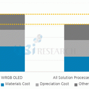
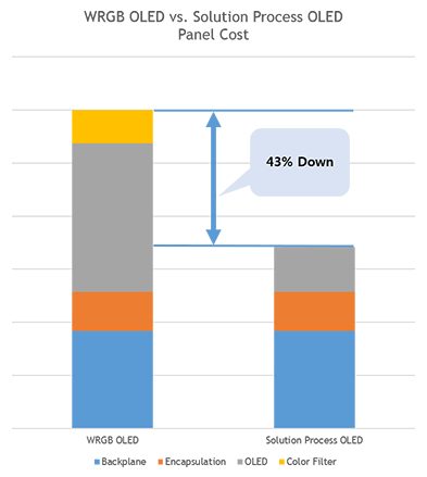
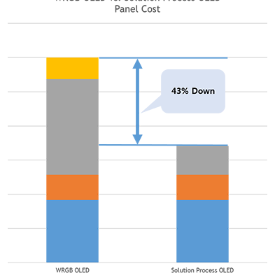
According to 2017 Solution Process OLED Annual Report published by UBI Research, when solution process (ink-jet printing) is applied to large area OLED, it could reduce up to 40% of component material cost, and approximately more than 18% of production cost compared to WRGB process that uses evaporation method.


Solution process is a technology that can manufacture RGB pixel structure of large size OLED panel without cutting mother glass using Gen8 manufacturing equipment or larger.


UBI Research analyst Hyunjun Jang explained that the solution process applied OLED has a simpler panel structure with 5 layers compared to 20 layers of WRGB OLED. WRGB OLED process material usage efficiency is only at 40% but solution process application could increase this to over 90%. Jang added that the lack of color filter is a factor that could decrease panel production price by reducing development cost. Particularly, this can greatly reduce emitting materials usage which occupies much of materials cost and contribute considerably to the fall in production cost. Furthermore, he added that cost setting of soluble emitting material per gram will be an important factor in production cost decrease and emphasized that organic material usage greatly decreases when soluble emitting materials are used but must consider price increase due to solvent cost, production cost, and development cost.


Solution process technology continues to receive attention as a key technology that can lead popularization of large area OLED, and key AMOLED panel companies are carrying out development.


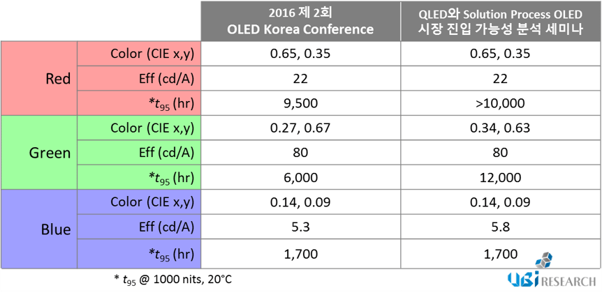
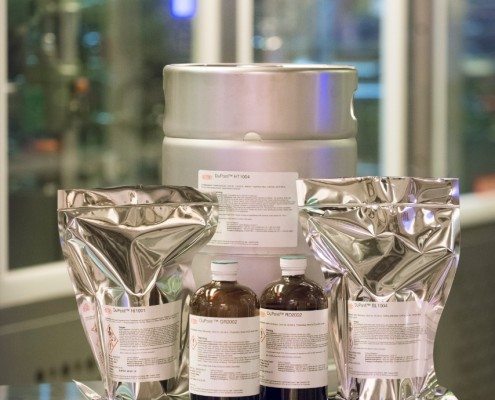
In terms of technology, solution process OLED has lower emitting efficiency and short lifetime as diverse solvent is added to existing evaporation materials to transform into ink leading to low purity. This has been an important issue for panel and material companies for past several years. To improve this, DuPont, Merck, Sumitomo Chemical and others have been actively developing soluble OLED emitting materials. Much like evaporation materials, blue materials showed particular difficulty in performance improvement. However, at present significant portion of technology development has been carried out and investigation shows approximately 80% of lifetime and efficacy of has been achieved compared to evaporation materials.


2017 Solution Process OLED Annual Report compared and analysed WRGB OLED and solution process OLED’s competitiveness in terms of process, materials, and cost. Key issues, soluble OLED emitting materials development status, key companies’ trend, and solution process OLED market are analysed from various perspectives.

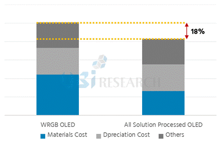
<Source: WRGB OLED and solution process OLED production cost comparison, UBI Research 2017 Solution Process OLED Annual Report>


Solution Process OLED, WRGB 보다 최대 40% 부품소재비용 절감 가능.

유비리서치에서 발간한 “2017 Solution Process OLED Annual Report”에 따르면 solution process(ink-jet printing)공정을 대면적 OLED에 적용시 현재 양산에 사용중인 증착방식을 적용한 WRGB 공정대비 최대 40%의 부품소재 비용, 약 18%이상의 제조원가 절감 가능성이 있는 것으로 분석했다.

Solution process는 대면적 OLED panel을 Gen8 이상의 장비에서 원장 분할 없이 RGB pixel 구조로 제조할 수 있는 기술이다.

유비리서치 장현준 선임연구원은 “Solution process가 적용된 OLED는 20 Layer 적층구조로 이루어진 WRGB OLED에 비해 5 Layer만으로 이루어져 패널 구조가 단순하다. WRGB OLED 공정은 발광재료 사용 효율이 약 40%에 불과한데 반해 Solution process 적용시 90% 이상으로 발광재료 사용 효율을 향상시킬 수 있다. 따라서 발광재료 사용량을 크게 감소시킬 수 있어 원가절감에 큰 기여를 할 것으로 기대된다. 또한 color filter를 사용하지 않는 것 또한 패널 제조 원가를 감소 시킬 수 있는 요인이다”라고 언급하였다. 이에 덧붙여 “ Soluble 발광재료 kg당 가격책정이 “원가절감”에 중요한 부분이 될 것이며, soluble 발광재료 사용시 유기재료 사용량은 크게 감소 하지만 solvent 비용과 제조비용, 개발비용으로 인한 가격상승 역시 고려해봐야 할 점”이라고 강조했다.

Solution Process 공정기술은 대면적 OLED의 대중화를 이끌 수 있는 핵심 기술로서 지속적으로 주목받고 있으며 주요 AMOLED panel 업체들 개발을 진행 중에 있다.

기술적인 관점에서 보면 solution process OLED는 기존 증착재료를 ink화 시키기 위해 다양한 solvent를 섞는다. 이때문에 증착재료보다 순도가 낮아 발광효율이 떨어지고 수명이 낮다. 이는 지난 몇 년간 panel 업체들과 재료업체들의 주요 과제였으며 이를 개선하기 위해 DuPont과 Merck, Sumitomo Chemical 등에서 적극적으로 soluble OLED 발광재료를 개발해왔다. 특히 증착재료와 마찬가지로 blue 재료의 성능개선에서 어려움을 겪어왔으나 현재는 상당부분의 기술 개발이 이루어져와 증착재료 대비 약 80% 수준의 수명과 효율을 확보한 것으로 나타났다.

이번에 발간된 2017 Solution Process OLED Annual Report에서는 WRGB OLED와 solution process OLED의 경쟁력을 공정, 재료, cost 측면에서 비교분석하였으며, 핵심이슈와 soluble OLED 발광재료 개발 현황과 주요 업체 동향, solution process OLED 시장을 다양한 관점에서 분석하였다.

<WRGB OLED와 solution process OLED 제조 원가 비교, UBI Research “2017 Solution Process OLED Annual Report”>


When 55inch OLED TV below US$ 1,000 will be realized?

At an analytical seminar on market entry potential of OLED and Solution Process OLED having been held in Small& Medium Business Center on October 14th, Manager Jeong Seong-jin of DuPont had time of introducing tendency regarding soluble OLED material and contents of the latest development.
Manager Jeong said that soluble OLED material and processing technology were on the verge of completion, but problems about how to complete Solution Process by combining it was still remained as issues, and also stated that Material performance (T95>9k hr, CE>25 cd/A) and Uniform printing (SRU>0.95), Contain (performance 90% of flood print), Conformal Drying (luminance aperture>95%) would be key elements.

1610191_1

<4 key elements to make commercialization of Solution Process>

Dupont progressed R&D on Solution Process previously by utilizing Nozzle Printing method that used Surface Energy Modification. This method had merits such like controlling quantity was easy and the nozzle was not clogged up due to constant supply of solution, there were limitations according to panel material together with a lot of raw material consumption.
Dupont lighted up a fact that R&D has been progressed to the direction of deposing organic materials after forming Bank with Ink Jet Printing method owing to such problems and Ink Jet market having been enlarged recently, and then opened Ink Jet Material performance.
When comparing with datum pronounced in 2016 2nd OLED Korea Conference by Dupont, the life seems to be developed for Red and Green in priority, and efficiency for Blue. Approximately 6% of Red life and two times of Green were improved, and about 10% of Blue efficiency was turned out to be increased.
Manager Jeong Seong-jin put emphasis by saying “In order to expand market to OLED from display market having been enlarged gradually, adoption of Solution Process is essential, and concentration for developing soluble OLED luminescence material will be made so that 55inch OLED TV below US$ 1,000 could be produced massively until 2020 by using Solution Process in set makers.”

%ea%b7%b8%eb%a6%bc2

<Performance comparison with existing Ink Jet material of DuPont>

US$ 1,000 이하의 55inch OLED TV 가능 시점은?

10월 14일 여의도 중소기업회관에서 개최된 ‘QLED와 Solution Process OLED 시장 진입 가능성 분석 세미나’에서 듀폰의 정성진 부장은 soluble OLED material에 대한 동향과 최신 개발 내용을 소개하는 시간을 가졌다.

정성진 부장은 현재 soluble OLED material과 공정기술은 완성 단계에 있으나 이를 결합하여 Solution Process를 어떻게 완성하는가에 대한 문제는 여전히 이슈로 남아 있으며, 이에 대해서 Material performance (T95>9k hr, CE>25 cd/A)와 Uniform printing (SRU>0.95), Contain (performance 90% of flood print), Conformal Drying(luminance aperture>95%)가 핵심 요소임을 언급하였다.

1610191_1

<Solution Process 상용화를 위한 4가지 핵심 요소>

기존에 듀폰은 Surface Energy Modification을 이용하는 Nozzle Printing 방식으로 Solution process 연구개발을 진행했었다. 이 방식은 용액을 지속적으로 공급하기 양 조절이 쉽고 노즐이 막히지 않는 장점이 있었으나, 재료소모가 많고 panel 소재에 따른 제약이 있었다.

이러한 문제와 최근 커져가는 Ink Jet 시장으로 인해 듀폰은 Ink Jet Printing 방식으로 Bank를 형성한 후 유기물을 증착하는 방향으로 연구개발이 진행되고 있음을 밝히며, Ink Jet Material Performance를 공개하였다.

듀폰이 2016년 제 2회 OLED Korea Conference에서 발표한 자료와 비교해 볼 때, Red와 Green은 수명을 Blue는 효율을 중점적으로 개발한 것으로 보인다. Red의 수명은 약 6%, Green의 수명은 2배 향상되었으며, Blue의 효율은 약 10% 증가한 것으로 나타났다.

정성진 부장은 “점차 대형화 되는 display 시장에서 OLED로 시장 확대를 하기 위해서는 Solution Process를 채용이 필수적이며, 세트 업체에서 solution process로 2020년까지 US$ 1,000 이하의 55inch OLED TV를 양산할 수 있도록 soluble OLED 발광재료 개발에 집중할 것.” 이라 강조하였다.


1610192_1

<듀폰의 기존 Ink Jet Material와의 Performance 비교>


Solution process OLED panel, LCD보다 저렴하게 제작 가능

유비산업리서치에서 14일 발간한 “2015 Solution Process OLED Report”에 따르면 “Solution process로 55inch OLED panel을 현재 양산되고 있는 WRGB 방식의 OLED panel보다 약 43% 저렴하게 제작할 수 있다.”라고 분석했다.

보고서에서는 “2015년도 2사분기 기준 55inch UHD OLED panel 가격과 수율을 기준으로 분석한 수치로서 현재 55inch UHD LCD panel의 제조 원가보다는 약간 높게 나타났다. 하지만 solution process OLED의 구조가 단순화 될 것이라는 점과 backplane과 encapsulation 수율이 개선될 수 있는 점을 고려해보면 LCD panel보다 저렴하게 제조할 수 있을 것”이라고 덧붙이며 solution process OLED가 대면적 OLED panel의 가격경쟁력을 확보할 수 있는 대안이 될 것이라고 밝혔다.

Solution process는 대면적 OLED panel을 Gen8 이상의 장비에서 원장 분할 없이 RGB pixel 구조로 제조할 수 있는 기술이며 주요 AMOLED panel 업체에서 적극적으로 개발을 진행 중에 있다.

하지만 solution process에 적용되는 발광재료는 기존 증착재료를 ink화를 시키기 위해 solvent를 섞기 때문에 증착재료보다 순도가 낮아 발광효율이 떨어지고 수명이 낮을 수 밖에 없다. 그럼에도 불구하고 solution process를 주요 panel 업체들에서 적극적으로 개발하고 있는 이유는 color filter를 사용하지 않고 발광재료 사용효율이 높으며 WRGB방식의 OLED panel에 비해 구조가 단순하기 때문에 원가절감을 할 수 있다는 점이다.

Solution process를 적용한 OLED panel은 Panasonic에서 가장 적극적으로 개발을 진행해왔으며 CES와 IFA에서 여러 차례 공개한 적이 있다. BOE와 AUO도 ink-jet 장비를 이용한 solution process OLED panel을 공개한 바 있으며 CSOT에서도 기술개발 방향을 solution process로 검토 중에 있다. AMOLED 산업의 선두주자인 Samsung Display와 LG Display에서도 적극적으로 개발을 진행 중이다. LG Display는 Gen8 ink-jet 장비를 도입하였으며 Samsung Display도 ink-jet 장비업체들을 중심으로 solution process OLED panel 개발에 본격적으로 착수한 상태이다.

Panel 업체뿐만 아니라 재료와 장비업체들도 solution process 기술개발과 상용화에 앞장서고 있다. Kateeva와 Sumitomo Chem., Merck와 Seiko Epson은 기술 협업을 맺었으며 DuPont는 soluble OLED 재료 생산시설 규모를 늘리고 가동을 시작했다고 최근 밝힌 바 있다.

이처럼 solution process 기술 개발과 상용화에 panel 업체뿐만 아니라 주요 재료, 장비업체들이 참여함에 따라 solution process OLED panel 시장은 빠른 시일 내에 성장할 것으로 기대된다.

“2015 Solution Process OLED Report”에서는 solution process OLED panel 시장이 2018년부터 본격적으로 양산되기 시작하여 2020년 약 US$ 2,329 million 규모로 성장할 것으로 전망했다.

Solution process OLED 핵심이슈는?

10월 7일 서울 the K 호텔에서 개최된 2015 Display Printed Electronics Seminar에서 단국대 진병두 교수와 한국 화학 연구원 이재민 박사는 각각 인쇄공정 OLED/PLED 소자 기술적 이슈와 용액공정 OLED 소재 기술 동향이라는 주제로 solution process OLED의 핵심 이슈를 되짚는 시간을 가졌다.

진병두 교수는 현재 solution process에 사용되는 재료 중 red, green는 효율과 수명 측면에서 많은 진보가 이루어졌지만 blue는 효율과 수명이 다른 두 색보다 낮다고 지적하며 red와 green만큼의 효율과 수명을 가지지 못한다면 blue 구현뿐만 아니라 white 구현이 힘들기 때문에 제대로 된 panel의 성능을 발휘하기 힘들다고 발표하였다.

이재민 박사는 진공증착 OLED는 재료의 합성과 정제만으로 재료 부분의 연구 개발이 가능한 반면, solution process OLED는 어떻게 잉크화를 시킬 것이냐에 대해서도 고려해야 한다고 밝히며 이런 이유로 재료 업체와 잉크화 관련 업체 사이에 다양한 collaboration이 나오고 있다고 발표하였다.

이 날 진병두 교수와 이재민 박사는 solution process OLED 기술의 핵심은 재료 특성 개발에 있다고 입을 모았다. Sumitomo Chem.과 DuPont에서 발표한 soluble 발광재료의 특성에 따르면 red와 green 재료 특성은 증착공정 OLED를 빠르게 따라잡고 있지만 blue 재료 특성은 이에 못 미치고 있는 것으로 나타났다. 이런 단점에도 불구하고 solution process OLED는 Gen8이상의 장비에서 대면적 OLED panel을 RGB 방식으로 양산할 수 있는 주요 기술이기 때문에 앞으로도 solution process에 대한 지속적인 연구개발이 이루어질 전망이다.

듀폰디스플레이, 앞으로의 TV 시장을 위한 OLED 재료 시설 가동 발표

지난 9월 30일(현지시간), 듀폰디스플레이는 대면적에 적용할 수 있는 용액공정용 OLED 재료에 대한 생산시설 규모를 늘리고 가동을 시작했다고 발표했다.

듀폰의 OLED재료는 OLED 디스플레이를 더 밝고, 더 선명하고, 지속 시간도 길면서 현재 OLED TV 패널보다 저렴하게 개발할 수 있도록 설계되었다. 새로 가동을 시작한 시설은 듀폰의 본사 소재지 미국 Wilmington 근처인 Newark의 DuPont Stine-Haskell 연구센터에 있다.

듀폰디스플레이의 글로벌 사업부장인 Avi Avula는 “OLED 재료는 OLED TV 성능에 매우 중요한 요소이다. 듀폰이 현재 시장에서 가장 뛰어난 용액공정 OLED 재료를 가지고 있다.”고 말했다. 또한 “우리의 비전은 OLED가 디스플레이의 표준이 되는 것이고, 이를 실현시키기 위해서는 2020년까지 대면적 OLED TV용 패널단가를 $ 1,000 이하로 생산하는 것에 초점을 맞추고 있다.”고 덧붙였다.

한편 듀폰디스플레이는 올해 용액공정 재료 성능으로 red 효율은 22 cd/A, green은 70 cd/A, blue는 5.5 cd/A를 표했으며, 이는 증착 재료에 비해 각각 76%, 82%, 11% 수준이다.

DuPont Displays Opens OLED Materials Scale-Up Facility for Next Generation TVs

On 30 September (local time), DuPont Displays announced the opening of a state-of-the-art, scale-up manufacturing facility designed to deliver production scale quantities of advanced materials that enable large-format, solution-based printed OLED displays.


These materials are designed to help manufacturers develop OLED displays that are brighter, more vivid, longer lasting and significantly less expensive than the OLED TVs on the market today.  The facility is located at the DuPont Stine-Haskell Research Center (Stine-Haskell) in Newark, Del., near DuPont’s global headquarters in Wilmington, US.


DuPont’s new scale-up facility is sized to meet the future growth expectations of the OLED TV industry, which analysts predict will increase by over 70 percent for the next several years and will require large quantities of highly sophisticated OLED materials. This new OLED facility at Stine-Haskell has large-scale formulation systems and can support simultaneous production of multiple product lines.


“Materials are critical to the performance of an OLED TV and we are confident that DuPont has the best performing solution OLED materials available in the market today,” said Avi Avula, global business director, DuPont Displays.  “Our vision is that OLEDs will become the display standard and to make that vision a reality, we are focused on helping our customers bring the cost of large sized OLED TVs down to less than $1000 by 2020.”

Portfolio Items