OLEDON, ‘초격차’ OLED 제조용 면소스 증착기술 공개

2018년 10월 24일부터 서울 코엑스에서 열리고 있는 IMID2018에서 OLED 증착장비 개발 벤처회사인 OLEDON이 ‘경쟁 국가들과의 초격차를 유지하기 위한’ OLED 제조 기술인 면소스 증착기술을 공개하여 이목을 집중시키고 있다.

OLEDON의 황창훈대표는 “한국이 현재의 OLED 생산국 1위를 앞으로도 유지하려면 창의적인 증착 기술개발 도전에 적극 투자하여야 한다”며, “미래의 중소형 및 대형 OLED 제조는 모두 면소스 증착기술이 사용될 것”이라 전망했다.

OLEDON이 세계최초로 개발 중인 곡면소스 FMM 증착기술은 2250ppi의 AMOLED 제조가 가능한 초고해상도 OLED 증착기술로서, 미세 패턴의 섀도우거리가 0.18um까지 가능하여 11K급 초고해상도의 AMOLED 패턴공정이 가능하다.

기존의 FMM 증착 패턴(좌)와 면소스 FMM 증착 패턴(우), Source: OLEDON

황 대표는 이러한 공정을 800ppi 섀도우 마스크로 확인한 결과, 면소스로 증착한 패턴의 발광면적이 기존의 증착 방법보다 1.7배 향상되었다고 발표하였다.

한편, OLEDON은 면소스 FMM증착기술의 원천특허를 보유하고 있으며 최근에는 대면적 OLED TV 제조용 수직형 면소스증착 특허를 출원하기도 하였다.

OLED TV 제조용 수직형 면소스 증착, Source: OLEDON


[SID 2018] OLEDON, presented about X-mixing plane source deposition technology for AMOLED efficiency enhancement.

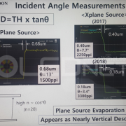
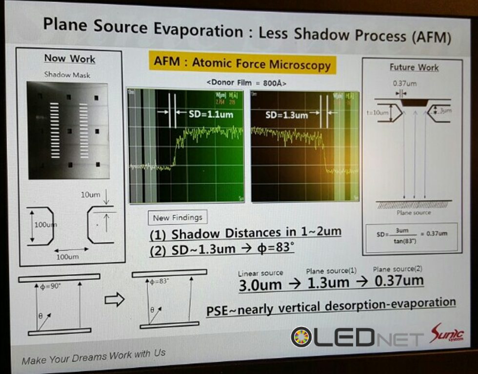
In SID 2018, Hwang Chang-Hoon, CEO of OLEDON, announced a new plane source FMM deposition technology that can produce ultra-high resolution AMOLED of 2,250 ppi.

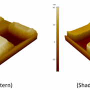
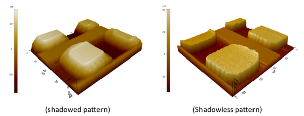
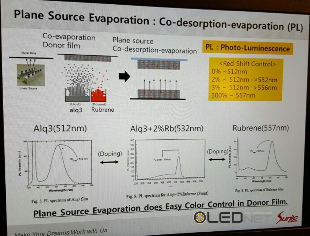
According to the announcement, the linear source currently applied to mass production has a problem of causing superimposition of fine adjacent patterns in a high resolution implementation due to a shadow distance of 3 μm. But Hwang said he succeeded in reducing the shadow distance of the patterns by 0.18 um using plane source, which is the smallest shadow distance ever introduced.

<Shadow effect comparison between current process and the process applied with the plane source, Source: OLEDON>

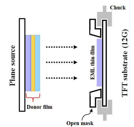
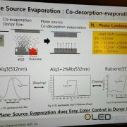
Hwang added that he developed ‘X-mixing’ technology in which the host and dopant thin films were separately deposited on the metal surface and then the host molecules and dopant molecules were automatically diffused through the plane evaporation to form the light emitting layer. Hwang commented, “It is not easy to control the composition of the dopant by using the linear source evaporation technology, which vaporizes the host material and the dopant material at the same time. However, since X-mixing technology can control the composition, it is possible to achieve a material utilization rate up to 4 times higher than the conventional method.”

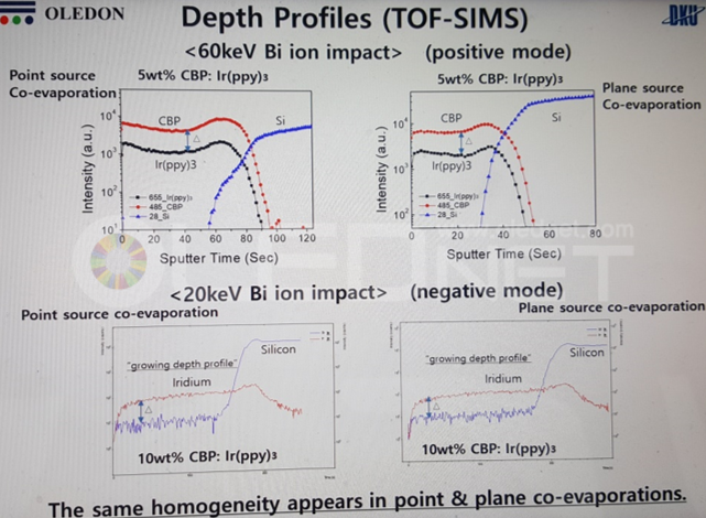
<SIMS data comparison between the emitting layer deposited by conventional method and the emitting layer deposited by the plane source, Source: OLEDON>

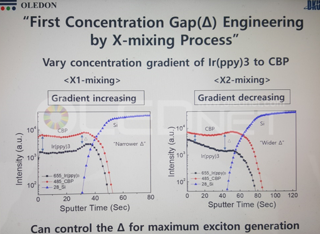
<Dopant gradient data of the emitting layer applied with X-mixing technology, Source: OLEDON>

Hwang said, “In case of green OLED produced by X-mixing technology, 40% improvement in the emitting efficiency was verified, compared to the existing technology. OLEDON is currently under development of the optimized X- mixing development for forming exciton and the mask aligner with new concept sub-micron precision.

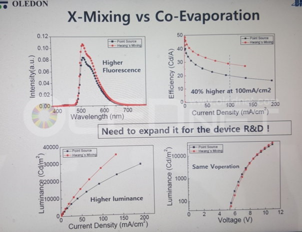
<Luminance data for green OLED produced by X-mixing technology and green OLED produced by the conventional method, Source: OLEDON>

Finally, Mr. Hwang mentioned that based on the development results, he plans to install a plane source FMM evaporator capable of manufacturing ultra-high resolution micro OLED devices in Dankook University.  (Reference: OLEDON homepage: www.oledon.co.kr)

[SID 2018] OLEDON, AMOLED 효율 향상용 X-mixing 면소스 증착 기술 발표

SID 2018에서 OLEDON의 황창훈 대표는 2,250ppi의 초고해상도 AMOLED를 제작 할 수 있는 새로운 면소스 FMM 증착기술을 발표했다.

발표에 따르면, 현재 양산에 적용 중인 리니어 소스는 3um의 섀도우 거리(shadow distance)로 인해 고해상도 구현 시 미세 인접 패턴들의 중첩을 발생시키기는 문제가 발생한다. 하지만 황대표는 면소스를 이용해 패턴들의 섀도우 거리를 0.18 um까지 줄이는데 성공하였다고 밝혔으며, 이는 현재까지 발표 된 섀도우 거리 중 가장 최소의 섀도우 거리라고 설명했다.

<기존 공정과 면소스를 이용한 공정의 섀도우현상(shadow effect) 비교, Source: OLEDON>

아울러 황대표는 호스트박막과 도판트박막을 따로 금속면에 증착 한 후 면증발을 통해 호스트 분자와 도판트 분자가 자동 확산되어 발광층이 형성되는 ‘X-mixing’기술을 개발하였다고 발표하였다. 황대표는 “기존 기술인 호스트 물질과 도판트 물질을 동시에 기화되는 리니어 소스 증착기술로는 도판트의 조성 제어가 쉽지 않으나, X-mixing 기술은 조성 제어가 자유자재로 가능하기 때문에 기존 대비 4배까지 향상 된 물질 사용률 달성이 가능하다”고 밝혔다.

<기존방식으로 증착 된 발광층과 면소스로 증착 된 발광층의 SIMS 데이터, Source: OLEDON>

<X-mixing 기술로 얻은 발광층의 dopant gradient 데이터, Source: OLEDON>

황대표는 “X-mixing 기술로 제작한 green OLED의 경우 기존 기술보다 40% 향상 된 발광효율을 확인하였다”고 언급하며 “OLEDON은 현재 소자의 발광효율향상을 목적으로 엑시톤형성의 최적화 된 X-mixing 개발과 신개념의 sub-micron 정밀도를 지닌 mask aligner를 개발 중”이라고 밝혔다.

<X-mixing 기술로 제작 된 green OLED와 기존 방식으로 제작 된 green OLED의 발광 데이터, Source: OLEDON>

마지막으로 황대표는 이번 개발결과를 토대로 초고해상도 마이크로 OLED 소자의 제조가 가능한 연구용 면소스 FMM 증착기를 단국대학교내에 설치할 계획이라고 언급했다. (참고:OLEDON사의 홈페이지 www.oledon.co.kr)

Sunic System’s Successful Demonstration of 1.1um Shadow Distance, High resolution up to 1500 ppi

Sunic System announced at 2016 IMID Business Forum that it succeeded in implementing 1.1um shadow distance by using plane source evaporation and 100um shadow mask. 1.1um shadow distance is able to manufacture 1000ppi~1500ppi high resolution.

Plane source evaporation is a technology to evaporate OLED light-emitting material on metal plate, invert it, apply heat to the metal plate, and vertically evaporate OLED light-emitting material. When the shadow angle(Ф) of OLED light-emitting material evaporation is 90 degrees, the value of SD(Shadow distance, step height / tanФ) is zero (0) theoretically. So, it is possible to design thick and high resolution FMM, which means high-resolution AMOLED panel can be manufactured. This principle was announced for the first time at IMID 2016 Business Forum, attracting big attention.

Sunic System Dr. Hwang Chang-hoon said “If we lower step height up to 3um by reducing the thickness of shadow mask based on this result, 0.37um shadow distance would be possible, which means we can manufacture maximum 2250ppi(11K) high resolution AMOLED panel. Accordingly, we will put spurs to development of 0.37 shadow distance”.

Also, he announced that co-evaporation of host and dopant that had been thought to be impossible in plane source has been resolved using flashing evaporation. He also proved that if donor film goes through flashing evaporation after co-evaporation of host and dopant, host and dopant can co-evaporate, and color control becomes easier by controlling dopant ratio to manufacture donor film.

1611021

<Result of Color Control after applying Flashing Evaporation>

1611022

<Result of 1.1um Shadow Distance>

선익시스템 1.1um shadow distance 데모 성공, 1500 ppi까지 구현 가능

선익시스템은 2016 IMID Business forum에서 plane source evaporation과 100um두께의 shadow mask로 1.1um의 shadow distance 구현에 성공했다고 발표했다. 1.1um의 shadow distance는 약 1000ppi~1500ppi의 고해상도 제작이 가능한 수치이다.

Plane source evaporation은 metal plate에 OLED 발광재료를 증착하고 뒤집은 후 metal plate에 열을 가함으로써 OLED 발광재료를 수직으로 증착시키는 기술이다. OLED 발광재료가 증착되는 shadow angle(Ф)이 90도가 되면 이론적으로 SD(Shadow distance, step hight / tanФ) 값이 0이 되기 때문에 FMM의 두께를 얇고 고해상도로 설계할 수 있어 고해상도 AMOLED panel 제조가 가능해 진다는 원리로서 지난 IMID 2016 학회에서 처음 발표되어 큰 관심을 끌었었다.

선익시스템의 황창훈 박사는 “이번 결과를 바탕으로 shadow mask 두께를 감소시켜 step height를 3um까지 감소시킨다면 0.37um의 shadow distance를 구현 가능하게 되고 이는 최대 2250ppi(11K)의 고해상도 AMOLED panel 제조가 가능해질 것” 이라며 0.37 shadow distance 구현을 위한 개발에 박차를 가할 것이라고 발표했다.

또한 이번 발표에서는 plane source에서는 불가능 할 것으로 예상됐던 host와 dopant의 co-evaporation을 급속가열(flashing evaporation)을 적용하여 해결 했다고 밝혔다. Donor film에 host와 dopant를 동시 증착한 후 donor film을 flashing evaporation을 하게 되면 host와 dopant를 동시에 증발시킬 수 있으며, donor film을 제작할 때 dopant ratio를 control 함으로써 color control을 쉽게 할 수 있음을 증명하였다.

1611021

<Flasing evaporation을 적용한 color control 결과>


1611022

<1.1um의 shadow distance를 구현한 결과>