JOLED, solution process OLED 후공정 양산 라인 구축 시작

JOLED가 중형 크기의 solution process OLED 양산을 위해 후 공정 라인을 치바 사업소에 구축한다고 발표했다. JOLED의 solution process OLED는 노미 사업소에서 TFT 공정부터 인쇄 공정까지인 ‘전 공정’이 진행된 뒤, 치바 사업소에서 모듈 공정과 최종 검사까지 진행되는 ‘후 공정’이 실시된다.

JOLED는 월 22만대 생산량을 목표로 하고 있으며, 2020년에 치바 사업소와 노미 사업소를 동시에 가동할 계획이다.

JOLED의 solution process OLED는 자동차와 하이엔드 모니터 시장을 타겟으로 하고 있으며, 크기는 10~32인치 범위이다.

한편, JOLED는 2018년 12월 5일부터 7일까지 일본 도쿄에서 열린 28TH FINETECH JAPAN에서 e-sports용과 의료 분야용 전문 21.6인치 FHD OLED 모니터, 자동차용 12.3인치 HD OLED와 12.2인치 FHD flexible OLED 등 다양한 중형 크기의 solution process OLED를 선보인 바 있다.

ASUS. 최초의 solution process OLED 상용화 모니터인 ‘PQ22UC’ 판매 시작

ASUS가 JOLED의 solution process OLED가 적용된 모니터인 ‘PQ22UC’를 호주와 영국에서 판매를 시작한다.

<Asus의 ‘PQ22UC’, Source: asus.com>

2018년에 열린 CES 2018에서 공개된 ‘PQ22UC’는 최초로 상용화 된 solution process OLED 모니터라는 점에서 많은 주목을 받았다.

‘PQ22UC’의 크기는 21.6인치이며 해상도는 4K(204ppi), 휘도는 140 nit/330 nit(일반/최대), 응답시간은 0.1 ms, 명암비는 1,000,000:1이다.

또한, 접이식 스탠드와 접이식 보호케이스가 제공되며 1 kg 미만의 무게로 인해 쉽게 휴대가 가능하다는 장점이 있다. 이러한 장점들로 외부에서 사진 작업이나 영상 촬영 등 전문적인 작업을 주로 하는 사용자들에게도 유용할 것으로 보인다.

현재 영국과 호주의 셀렉트 샵(select shop)에서의 가격은 세금포함 각각 £4,699와 €5,160 수준이다. 모바일 기기와 TV에서 점유율을 확대해 가고 있는 OLED가 모니터 시장에서도 점유율을 확대해 나갈 수 있을지 귀추가 주목된다.

What is the investment cost for large-area OLED that will lead the premium TV market?

■ Investment cost comparison and analysis for WRGB OLED, solution processed OLED and QD-OLED
■ Total OLED process equipment is expected to form a market of US$ 58.8 billion from 2018 to 2022, and inspection equipment market is estimated as US$ 8.4 billion

In the premium TV market, the market share of OLED TVs is steadily rising, and the number of OLED TV camps is gradually increasing. OLED TV adopts color filter to WRGB OLED, and currently LG Display only mass produces the OLED panels.

On the other hand, Samsung Display is developing QD-OLED (blue OLED + quantum dot color filter) to compete with WRGB OLED in the premium TV market. Blue OLED is a technology in which the blue light emitted from OLED passes through a quantum dot layer and a color filter to represent red and green colors.

<Expected structure of QD-OLED>

UBI Research analyzed the structure and investment amount of WRGB OLED and QD-OLED, which are the latest issues, in the‘AMOLED Manufacturing and Inspection Equipment Industry Report’ published on June 6. In addition, the investment amount of the solution process OLED, which has got the industry attention due to its possible implementation of real RGB in large-area OLED, is also analyzed and compared.

As a result of analyzing the equipment investment cost based on the 8th generation 26K, the QD-OLED investment cost is 3% higher than WRGB OLED and the investment cost of solution process OLED is 19% less than that of WRGB OLED.

In the QD-OLED investment cost, it is reflected that QD color filter is separately formed and its laminating process is added. For the analysis of solution processed OLED investment cost, color filter is excluded and ink-jet printer is applied instead of deposition equipment.

In addition, the report forecasts the overall OLED equipment market from 2018 to 2022. The total OLED overall equipment market is expected to reach US$ 106.7 billion from 2018 to 2022. The market for process equipment is projected as US$ 58.8 billion and inspection equipment market is to be US$ 8.4 billion.

Premium TV 시장을 주도할 대면적 OLED의 투자 비용은?

최근 premium TV 시장은 OLED TV의 점유율이 지속적으로 상승하고 있으며 OLED TV 진영도 꾸준히 증가하고 있는 추세다. OLED TV는 WRGB OLED에 color filter를 적용한 구조로써, 현재 LG Display만이 유일하게 OLED panel을 양산하고 있다.

이에 Samsung Display에서는 premium TV 시장에서 WRGB OLED에 대항하기 위해 blue OLED + quantum dot color filter(이하 QD-OLED)를 개발하고 있는 것으로 알려졌다. Blue OLED는 OLED에서 발광 된 청색광이 quantum dot층과 color filter를 통과해 red와 green 색을 나타내는 기술이다.

<QD-OLED 예상 구조>

유비리서치는 지난 6일 발간한 ‘AMOLED Manufacturing and Inspection Equipment Industry Report’에서 최근 이슈가 되고 있는 WRGB OLED와 QD-OLED의 구조와 투자 금액을 분석했다. 뿐만 아니라, 대면적 OLED에서 real RGB를 구현할 수 있어 주목받고 있는 solution process OLED의 투자 금액도 함께 분석하여 비교했다.

8세대 26K 기준으로 장비 신규 투자비를 분석한 결과, QD-OLED 투자비는 WRGB OLED에 비해 3%가 많고 solution process OLED는 WRGB OLED에 비해 19% 적은 것으로 조사되었다.

QD-OLED 투자비에서는 QD color filter가 따로 형성되고 이를 합착하는 공정이 추가된 내용이 반영되었으며, solution process OLED 투자비에서는 color filter가 제거되고 증착 장비 대신 ink-jet printer가 투입된 내용이 반영되었다.

이 밖에 본 보고서에서는 2018년부터 2022년까지 OLED 전체 장비 시장도 예상하였다. 2018년부터 2022년까지 OLED 전체 장비 시장은 US$ 106.7 billion을 형성할 것으로 전망되며, 공정 장비는 그 중 US$ 58.8 billion, 검사 장비는 US$ 8.4 billion의 시장을 형성할 것으로 예상된다.

<2018년~2022년 장비별 전체 시장 점유율 전망>

JOLED, Production of medium sized solution process OLED in 2020

JOLED announced that it will mass-produce mid-size solution processed OLED applicable to automobiles and monitors in 2020.

On June 26, JOLED, a subsidiary of Japan Display, said that it will open a ‘JOLED Nomi Office’ in Nomi City, Ishikawa prefecture on July 1 with the operation target in 2020.

<JOLED Nomi Office, Source: j-oled.com>

The flagship product is expected to be a medium sized (10 ~ 32 inch) solution process OLED for automobiles and high-end monitors.  At the 2018 OLED Korea conference held by UBI Research in last March, Toshiaki Arai, chief technologist of JOLED said that it would target the middle-sized OLED market with solution process OLED.

<JOLED development roadmap, announced at the 2018 OLED Korea conference>

JOLED, 2020년 중형 solution process OLED 양산

JOLED가 2020년 자동차나 모니터용에 적용 가능한 중형 크기의 solution process OLED를 양산한다고 밝혔다.

6월 26일 Japan Display의 자회사 JOLED는 7월 1일 이시카와현 노미시에 ‘JOLED 노미 사업소’를 개설하고 2020년 가동을 목표로 하고 있다고 밝혔다.

JOLED 노미 사업장은 Japan Display의 기존 노미 공장 위치에 설립되어 기존 설비를 이용하는 것 외에도, solution process OLED 양산을 위한 추가 설비 등의 새로운 건물이 지어질 예정이다. 규모는 지상 5층에 부지 면적은 약 10 만 평방 미터로, 5.5세대 (1300mm × 1500mm) 유리 기판 기준으로 월 생산 약 2 만장의 생산 능력을 갖출 예정이다.

<JOLED 노미 사업소, Source: j-oled.com>

주력 생산 제품은 자동차나 하이 엔드 모니터용 중형 (10~32 인치) solution process OLED로 예상 된다. 지난 3월에 유비리서치가 개최 한 2018 OLED Korea conference에서 Toshiaki Arai chief technologist는 solution process OLED로 중형 OLED 시장을 공략할 것을 밝히기도 했다.

<2018 OLED Korea conference에서 밝힌 JOLED의 개발 로드맵>

In order to accelerate the mass production of solution processed OLED?

At the latest OLED technology trends seminar organized by UBI Research in Seoul COEX on April 26th, professor Seo presented about the status of solution processed OLED for large-area TV production.

Professor Seo emphasized that there are four technical challenges to advance the mass production of solution processed OLED.


The first challenge is the development of materials that can form stable and flat thin films. When the emitting material for solution process is applied, the solvent causes a convection phenomenon due to solubility and boiling point. Therefore, it is difficult to make a flat film because the speed at which the solvent flows is different for each region.


The second is the development of cross linked HTL materials. Emitting material companies are mixing cross-linking agents into HTL materials for solution process to solve intermixing problems between layers. However, a pinhole is formed due to a cross linking reaction with the surrounding small molecular materials when crosslinked materials in small molecule type are used. This kind of pinhole lowers the uniformity of the thin film, and therefore it is necessary to develop crosslinked HTL materials that can improve the reproducibility and lifetime of OLED in solution process.


The third is the jetting condition. He proposed a jetting condition that can minimize the volume deviation of the emitting material for solution process every head since it is necessary to drop the emitting material for solution process of less than 4 pl to the desired position in the size of 20-50 um to realize 8K. Lastly, he commented that it is required to optimize the drying process of solvent. UBI Research described that the solution OLED process has a simple (5 layer) structure and high material utilization efficiency compared to the conventional deposition process. In addition, it is possible to manufacture large-area OLED with RGB structure without the division of mother glass at Gen8 or higher. When major panel makers adopt solution process, it is available to reduce the manufacturing cost of OLED due to the decrease of equipment and equipment scale as well as material cost and labor cost reduction. According to the 2018 Annual OLED Display Industry Report and 2018 Emitting material Industry Report published by UBI research, solution processed OLED is to be mass produced from 2019 in earnest, and the shipment is expected to be 0.2 million units in 2019 and 9.2 million units in 2022. Accordingly, the emitting material market for solution process is estimated to grow to US$ 110 million in 2022 from US$ 9 million in 2019.

용액 공정용 OLED 양산을 앞당기기 위해서는?

지난 26일 코엑스에서 유비리서치가 개최한 OLED 최신 기술 동향 세미나에서 서민철 교수는 대면적 TV 제조를 위한 용액 공정용 OLED 공정 현황을 발표하였다.

서 교수는 용액 공정용 OLED의 양산을 앞당기기 위해서는 4가지의 기술과제가 남아있다고 강조하였다.

첫 번째 기술과제는 안정적이며, 평평한 박막을 형성할 수 있는 재료의 개발이다.

용액 공정용 발광재료가 도포 될 시, 용해도와 끓는점 등으로 인해 solvent는 대류 현상을 일으킨다. 이로 인해 각 영역마다 solvent가 날아가는 속도는 달라져 평평한 박막을 만들기 어렵다고 설명하였다.

두 번째는 가교형 HTL 재료의 개발이다.

발광재료 업체에서는 layer간 intermixing 문제를 해결하기 위해 용액 공정용 HTL 재료에 가교제를 혼합하고 있다. 그러나 저분자 계열의 가교형 물질을 사용할 경우, 주변의 저분자 물질과의 가교반응으로 인해 pinhole이 형성된다. 이러한 pinhole은 박막의 uniformity를 저하시키기 때문에 용액 공정 OLED의 재현성과 수명을 떨어트리기 때문에 이를 개선할 수 있는 가교형 HTL 재료의 개발이 필요하다고 언급했다.

세 번째는 jetting 조건이다.

서 교수는 4pl미만의 용액 공정용 발광재료를 20-50 um의 크기로 원하는 위치에 떨어트려야 8K를 구현할 수 있다며, head 마다 용액 공정용 발광재료의 부피 편차를 최소화 할 수 있는 jetting 조건이 요구된다고 말했다.

마지막으로 서 교수는 solvent의 건조 공정 최적화가 필요함을 언급하며 발표를 마쳤다.

유비리서치에 따르면, 용액 공정용 OLED 공정은 기존 증착 공정에 비해 OLED 구조가 단순(5layer)하며 재료 사용 효율이 높다. 또한, Gen8 이상에서 원장 분할 없이 RGB 구조의 대면적 OLED 제조가 가능하며, 주요 panel 업체가 solution process를 도입 할 시 설비 및 장비 규모 축소뿐만 아니라 재료비와 인건비 절감 등으로 OLED의 제조원가를 낮출 수 있다.

유비리서치는 2018 Annual OLED Display Industry Report와 Emitting material Industry Report를 통해 용액 공정용 OLED는 2019년부터 본격적으로 양산되어 2019년 20만 개, 2022년 920만 개 출하될 것으로 전망하였다. 이에 따른 용액 공정용 발광재료 시장은 2019년 900만 달러를 형성하여 2022년 약 1.1억 달러의 규모가 될 것으로 예상하였다.

Inkjet might take advantageous position for Gen11 super large OLED mass production line!

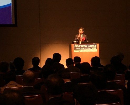
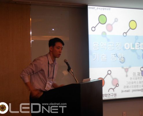
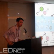
Toshiaki Arai, chief technologist of JOLED and James Lee, deputy chief engineer of TCL made presentations for the solution processed OLED on March 7 at the ‘4th OLED Korea conference’ held at Novotel Ambassador Hotel in Gangnam, Seoul, hosted by UBI Research.

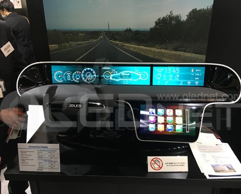
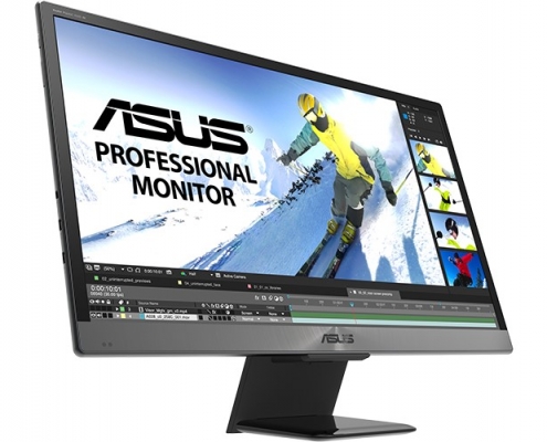
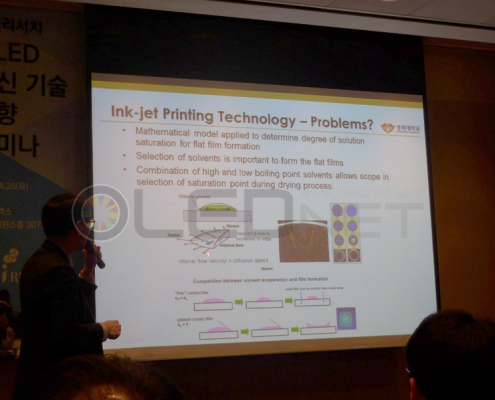
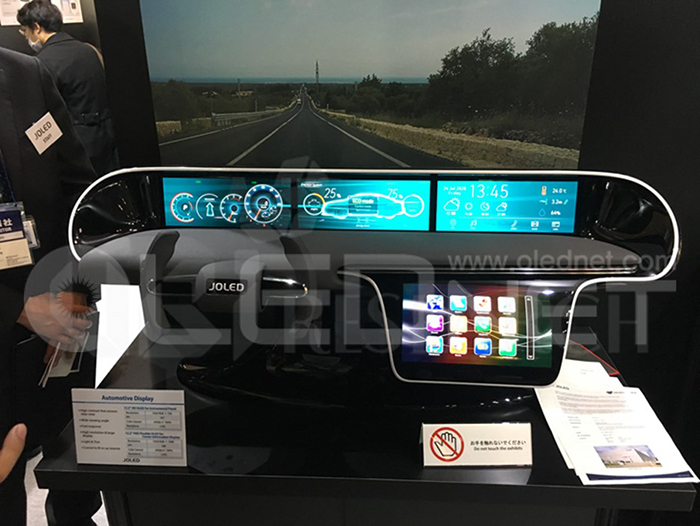
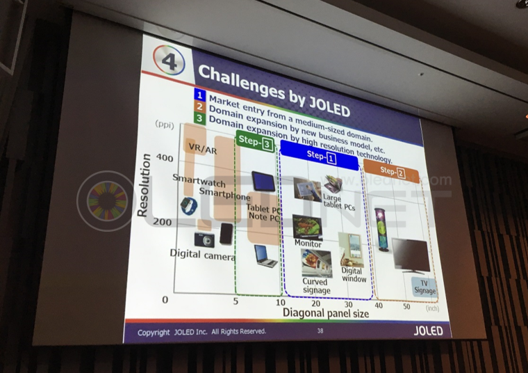
Toshiaki Arai, chief technologist of JOLED announced that JOLED will focus on the medium-size OLED market for 10 ~ 30 inch tablets with solution processed OLED. He explained “OLEDs for mobile devices are currently targeting over 500 ppi and at least 800 ppi, which is hard for today’s printing technology. However, current printing technology is competitive enough since the medium-size OLED for tablets is 300 ppi level”.

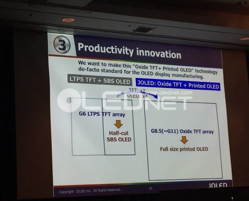
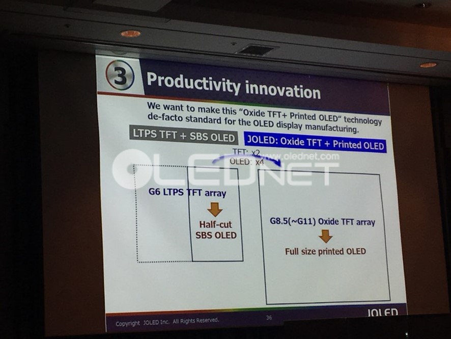
He also added, “While it is required to divide the mother glass with the deposition technology currently in use, JOLED’s oxide TFT and solution process OLED can be adopted to Gen 8.5 as well as Gen 11 without cutting the mother glass. Thus, we expect panel production to be increased significantly.

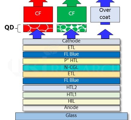
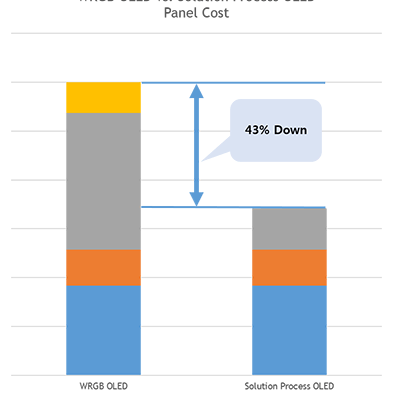
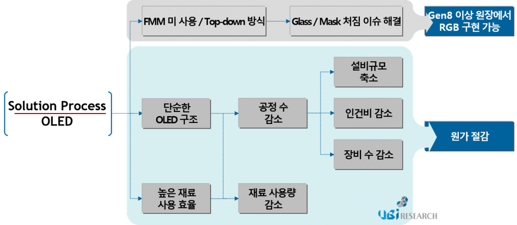
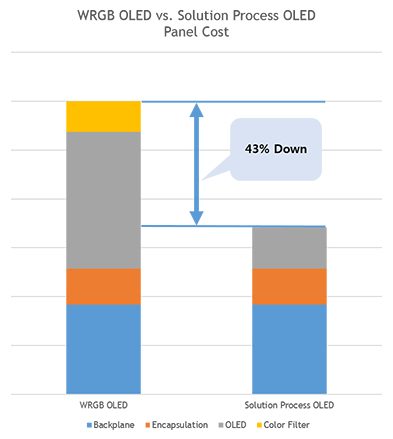
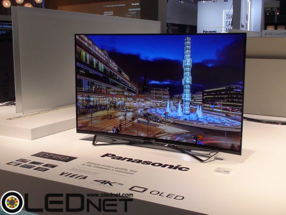
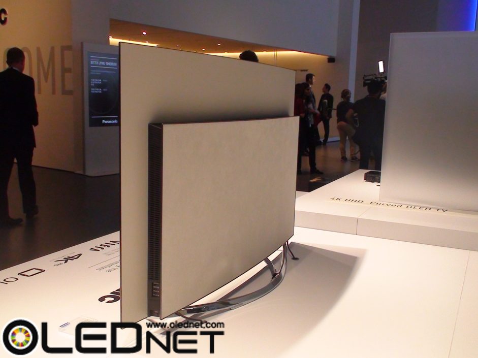
James Lee, deputy chief engineer of TCL commented that the next-generation premium TVs are to implement 70-inch or larger screen, full black representation, high-definition at 8K resolution, and design differentiation such as slim & flexible. He said “solution process technology enables large RGB OLED implementation, which can improve image quality and reduce cost by using less material. TCL is currently developing solution process technology, which might be expected to be applied to its planned Gen 11 factory. ”

He commented “OLED TV prices are now approaching the price of LCD TVs based on 65-inch standards. In 2021, OLED TVs and LCD TVs will not differ in price, and OLED TVs will become the mainstream of the premium TV market. ”

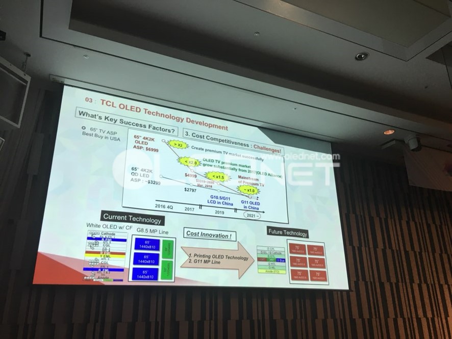
Also he emphasized “Gen11 OLED needs to improve mura (unevenness) free technology, but it can produce six sheets of 75-inch OLED panels, and it is three times the production volume of GEN 8.5, with a cutting efficiency rate of 95% or more. In order for OLED TV to become the mainstream of the TV market, it is necessary to establish Gen 11 solution process OLED factory. ”

Gen11 초대형 OLED 양산라인, inkjet으로 선점!

3월 7일 유비산업리서치 주최로 서울 강남 노보텔앰배서더 호텔에서 열린 ‘제 4회 OLED Korea conference’에서 JOLED의 Toshiaki Arai chief technologist와 TCL의 James Lee deputy chief engineer는 solution process OLED를 주제로 발표를 진행했다.

JOLED의 Toshiaki Arai chief technologist는 solution process OLED로 10~30 inch대 태블릿용 중형 OLED 시장을 집중 공략할 것을 밝혔다. Toshiaki Arai chief technologist는 “mobile 기기용 OLED는 현재 500 ppi를 넘어 최소 800 ppi 이상을 목표로 하고 있어 현재 프린팅 기술로는 힘들다. 하지만 태블릿용 중형 OLED는 300 ppi 수준이기 때문에 현재 프린팅 기술로는 충분히 경쟁력이 있다”고 설명했다.

이어서 “현재 적용 되고 있는 증착 기술은 원장 분할이 필수이지만, JOLED의 oxide TFT와 solution process OLED는 Gen8.5를 넘어 Gen11에서도 원장분할 없이 공정이 가능하기에 패널 생산량도 대폭 확대 될 수 있을 것”이라 전망했다.


TCL의 James Lee deputy chief engineer는 차세대 premium TV는 70 inch 이상의 대형 화면과 완벽한 블랙표현과 8K 해상도의 고화질, slim & flexible 등의 디자인 차별화 임을 언급하였다. James Lee deputy chief engineer는 “solution process 기술이 대형 RGB OLED 구현이 가능하여 화질 향상이 가능하고 적은 재료 사용으로 원가 절감에도 기여할 수 있을 것”이라며, “TCL은 현재 solution process 기술을 개발 중으로 Gen11 공장에 적용이 가능할 것으로 예상된다”고 밝혔다.

이어서 “현재 65 inch 기준 OLED TV 가격이 LCD TV 가격에 근접하고 있다”며 “2021년에는 OLED TV와 LCD TV 가격이 차이가 없을 것이며 OLED TV가 premium TV 시장의 주류로 자리잡을 것”이라 설명했다.

또한, “Gen11 OLED는 Mura free 기술 향상이 필요하지만, 75 inch OLED 패널을 6장 생산이 가능하며 Gen8.5 대비 3배 증가한 생산량과 95% 이상의 면취율이 가능하다”고 설명하며 OLED TV가 TV 시장의 주류로 자리잡기 위해서는 Gen11 solution process OLED 공장 건립이 반드시 필요할 것이라 강조했다.

UBI Research, publishes ‘2018 OLED Panel Industry Report’, which analyzes the indicators of OLED industry in 2017

UBI Research published ‘2018 OLED Panel Industry Report’ on February 12, 2018, which analyzes the indicators of OLED industry for the year of 2017.

This report seems very helpful to forecast OLED industry, which is most likely to become the main display in future, since it analyzes panel makers’ development trends, key issues, applied products, and relevant markets from various perspectives on rigid and flexible OLED as well as solution processed OLED.

In the report, the status of OLED products in 2017 is summarized into various applications such as smart phones and TVs, and the trends of newly released products and related issues can be identified.

According to the report, a full-screen smart phone, which has become a trend in recent years, can mainly be applied to flexible OLEDs, while rigid OLEDs using COG (chip on glass) are required to ensure module space at the top and bottom side. Therefore, it is expected that panel makers will implement full-screen as a notch type rather than a current rectangle type to improve the added value, and demand of rigid OLED, which is on the decrease.

Meanwhile, UBI Research predicts that shipment for rigid OLEDs will be 270 million units and that for flexible OLEDs will be 230 million units in 2018, generating sales of US$ 12.5 billion and US$ 23.9 billion, respectively.  Also, analysis shows that the solution process, capable of manufacturing large-area OLED panels with RGB structure without cutting mother glass at Gen 8 or higher generation, will be adopted at the mass-production from 2019. Consequently, 2 million units of solution processed OLED will be shipped in 2019 and 9.2 million units will be shipped in 2022.

<Flexible OLED shipment forecast>

유비리서치, 2017년 OLED 산업의 지표를 분석한 ‘2018 OLED Panel Industry Report’ 발간

유비리서치는 2017년 한해 동안의 OLED 산업 지표를 분석한 ‘2018 OLED Panel Industry Report’를 지난 12일 발간하였다.

본 보고서는 rigid부터 flexible, solution process OLED 전반에 대해 panel 업체 개발 동향, 핵심 이슈, 적용 제품현황, 시장 등을 다양한 관점에서 분석하여, 향후 디스플레이의 주력이 될 OLED 산업을 전망하는데 도움이 될 것으로 예상된다.

보고서에는 2017년 OLED 적용 제품현황을 스마트폰과 TV 등 여러 어플리케이션으로 나누어 출시 흐름과 이에 따른 이슈를 확인할 수 있다.

보고서에 따르면, 최근 트렌드로 자리 잡고 있는 full-screen smart phone은 flexible OLED만 적용 가능하며, COG(chip on glass)방식이 적용되는 rigid OLED는 상∙하부에 모듈 공간을 확보해야 하기 때문에 적용이 어렵다고 설명했다. 따라서, panel 업체는 감소하는 rigid OLED의 수요와 부가가치를 향상시키기 위해 현재의 모양(rectangle)보다는 notch type으로써 full-screen을 구현할 것이라 전망했다.

한편, 유비리서치는 2018년에는 Rigid OLED가 2.7억 개, flexible OLED가 2.3억개 출하되어, 각각 125억 달러, 239억 달러의 매출액을 형성할 것으로 전망하였다. 또한, Gen8 이상에서 원장 분할 없이 RGB 구조의 대면적 OLED panel 제조가 가능한 solution process는 2019년부터 본격적으로 양산되어 2019년 20만 개, 2022년 920만 개의 solution process OLED가 출하될 것으로 분석하였다.

<Flexible OLED 출하량 전망>

[iMiD 2017] TCL, Solution process OLED와 QLED에 개발 집중

TCL의 Xiaolin Yan CTO는 29일 부산 벡스코에서 열린 iMiD 2017 기조연설에서 white OLED TV 이후의 premium TV로 solution process OLED TV와 자발광 QLED TV를 언급했다.


Yan CTO는 현재 premium TV 시장을 주도하고 있는 white OLED TV는 QD LCD TV 대비 뛰어난 화질과 디자인 차별화, 고해상도 구현, 자연 친화적인 특성으로 premium TV의 모든 요구 조건을 충족하고 있다고 언급했다.

또한, 현재 QD LCD TV보다 높게 책정 되어 있는 가격도 solution process를 적용하면 극복이 가능할 것으로 예상하며 2019년에 대량 생산도 가능할 것으로 전망했다.

Yan CTO는 “solution process 공정은 원장 분할 없이 공정 진행이 가능하기 때문에 Gen 10.5에서 75 inch 패널 생산이 용이할 것”이라며 “뿐만 아니라 전면 발광 방식의 RGB OLED TV 생산도 가능할 것”이라 예측했다. 다만, 이를 위해서는 재료와 장비의 궁합과 잉크 형성 공정 기술 개발 등이 이루어져야 한다고 강조했다.


이어서 자발광 QLED TV를 언급하며 “QLED 구조는 OLED 구조와 매우 흡사하기 때문에 진입 장벽이 낮아 기술 적용이 용이할 것”라며 “현재 OLED 대비 blue 발광층의 수명과 효율이 매우 낮은점과 카드뮴 사용 없이 성능이 확보되어야 한다”고 언급했다.

마지막으로 solution process OLED TV와 자발광 QLED TV의 상용화를 촉진하기 위한 광동 JUHUA에 printing technology 설립을 언급하며 차세대 프리미엄 TV 개발을 위해서는 재료와 장비 업체, 패널 업체들의 협력이 필요하다고 강조했다.

[iMiD 2017] TCL, Development focusing on Solution process OLED and QLED

TCL’s Xiaolin Yan CTO addressed solution process OLED TV and self-emitting QLED TV as premium TV after white OLED TV at iMiD 2017 keynote address in BEXCO, Busan on 29th.


Yan CTO noted that white OLED TV, which is currently leading the premium TV market, meets all the requirements of premium TV due to its superior image quality, design differentiation, high resolution realization and nature-friendly characteristics compared to QD LCD TV.


In addition, the price that is higher than the current QD LCD TV is expected to be overcome by applying the solution process, and mass production is also expected in 2019.


Yan CTO predicted that the “solution process would be easy to produce 75-inch panels at Gen 10.5 because the process can be performed without splitting the ledger,” and “it is also possible to produce full-emission RGB OLED TVs.” However, he emphasized that the compatibility of materials and equipment and the development of ink forming process technology should be done.


Following to that, “QLED structure is very similar to OLED structure, so it is easy to apply the technology because of the low entry barriers,” he said. “The lifetime and efficiency of the blue light emitting layer compared to the current OLED is very low, and performance must be ensured without the use of cadmium.”


Lastly, He mentioned the establishment of printing technology in Guangdong JUHUA to promote the commercialization of solution process OLED TV and self-luminous QLED TV, and emphasized the cooperation of material, equipment and panel makers to develop next-generation premium TV.

Solution Process OLED 도입 예상효과는?

Solution process OLED는 발광층 재료들을 solvent에 녹인 후 용액화 하여 printing으로 형성한 OLED이다. 일본의 JOLED LG Display에서 가장 적극적으로 개발하고 있으며, 중국의 BOE CSOT에서도 개발을 진행중이다.

Solution process Gen8이상 원장에서 RGB pixel 구조의 대면적 OLED panel 구현이 가능하고, 재료사용효율이 높고 단순한 layer로 개발되고 있어 양산 성공 시 원가절감이 가능하다는 장점이 있다.

161221

Solution Process OLED 도입 시 기대 효과, “Market Entry Analysis for Solution Process OLED -The Possibilities and Opportunities Report”, UBI Research

하지만 soluble OLED 발광 재료의 효율과 수명이 증착재료 대비 낮다는 점과, OLED 구조와 재료가격이 정해지지 않은 점 등등의 다양한 이슈들이 존재하고 있다.

현재 대면적 OLED 시장은 WRGB 방식으로 프리미엄시장 공략의 전략을 펼치고 있지만 추후 LCDOLED로 대체하기 위해서는 저비용/고생산 기술이 핵심 요소이며, solution process OLED가 핵심기술이 될 것으로 예상된다.

대면적 OLED가 프리미엄 TV 시장에서 멈출지, 프리미엄 TV 시장에서 벗어나 중저가 TV시장까지 진출하여 LCD와 경쟁을 할지는 solution process OLED의 성공여부에 결정될 것으로 예상된다.


JOLED, 프린팅 OLED 박차…“19.3인치·12.2인치 개발완료, 2018년 양산”

JOLED의 토모아키 츠보카 이사(도쿄=OLEDNET)

JOLED의 토모아키 츠보카 이사(도쿄=OLEDNET)

강현주 기자 / jjoo@olednet.com

JOLED가 프린팅 기술 기반의 19.3인치, 12.2인치 OLED 패널 개발을 완료하고 2018년부터 양산에 들어간다.

4 6일부터 8일까지 도쿄에서 열린 파인테크 재팬 2016’의 스페셜 세션에서 JOLED의 사업개발부 수장인 토모아키 츠보카 이사는 혁신에 도전하는 JOLED의 전략이라는 제목으로 연설하며 이같이 밝혔다.

츠보카 이사에 따르면 JOLED는 최근 프린팅 기반의 12.2인치 FHD 플렉서블 OLED 패널과 19.3인치 4K OLED 패널 시제품 개발을 완료했다. 12.2인치 제품은 180ppi19.3인치 제품은 230ppi이다.

JOLED는 오는 8월부터 시제품의 양산 관련 검증 작업에 들어갈 계획이며 2018년부터는 정식으로 양산할 예정이다. 이를 위해 JOLED는 4.5세대 양산라인(730x920mm)을 준비 중이다.

JOLED는 그동안 스마트폰용 OLED 패널 양산이 주력이었던 업체다. 이 회사는 프린팅 기술을 기반으로 대형 부문에 진입함으로써 이를 성장 동력으로 삼는다는 전략이다.

츠보카 이사는 이날 세션에서 프린팅 방식의 OLED 양산 기술의 특징을 설명하며 JOLED만의 우수한 프린팅 기술을 내세웠다.

츠보카 이사는 “RGB 프린팅 방식은 대기 중 대형 OLED 패널 구현이 가능하며 작업과정이 짧은 게 장점이지만 얼룩(Mura) 개선 및 물질 특성 개선 등이 필요하다고 했다. 그는 “JOLED의 경우 독자적인 기술을 통해 많이 개선했다알고리즘 개선 및 재료, 디바이스 구조 최적화를 통해 많이 개선했다고 덧붙였다.

그는 “JOLED는 프린팅 기술력을 가지고 대형 패널 시장에 진입하려고 한다라며 “OLED는 높은 품질의 플렉서블(flexible), 프리폼(freeform), 투명(transparent) 등의 구현이 가능해 역, 공항, 미술관 등에 공간의 혁신을 가져다 줄 것이라고 강조했다.

한편 ‘파인테크 재팬 2016’은 4월 6일부터 8일까지 도쿄 빅사이트에서 진행된 디스플레이 기술 관련 전시회다. 올해로 26회째를 맞는 이번 행사에서는 SDC, LGD, BOE, JDI, JOLED 등 약 260여 업체가 참여한다.

키워드로 전망하는 2016 OLED 산업

  1. Flexible AMOLED Investment

2016년에는 Samsung Display와 LG Display, BOE, Japan Display의 flexible AMOLED 양산라인에 대한 투자가 본격적으로 이루어 질 것으로 예상된다. Samsung Display는 신규 Galaxy모델에 flexible AMOLED panel을 적용하기 위해서는 양산라인 투자가 필수적이며, Apple에 flexible AMOLED panel을 공급하게 될 경우 2016년에 투자될 flexible AMOLED 양산라인의 규모는 상당히 커질 것으로 예상된다. LG Display도 구미 P6 line에 flexible AMOLED line 장비 발주가 본격적으로 이루어 질 것으로 예상되며, 이외에 Apple의 요구에 따라 추가적인 flexible AMOLED 양산라인 투자가 있을 것으로 전망된다. Japan Display도 Apple의 flexible AMOLED 공급업체 후보로 투자가 가능할 것으로 예상된다. BOE는 청두의 Gen6 45K flexible AMOLED 양산라인에 대한 발주가 본격적으로 시작될 것으로 전망된다.


  1. P10

LG Display가 2015년 4분기에 신규공장 건설과 일부 설비투자에 1조8400억원을 투입한다고 밝히며, 투자의 첫 단계로 대형 패널을 생산할 수 있는 P10 line의 공장 부지 조성을 시작했다. 하지만 아직 투자 방향을 결정하지 않은 상태이다. P10의 투자 방향은 대형 LCD 패널만 생산하거나 대형 OLED 패널을 생산하는 방향, 중소형 OLED 패널만 생산하는 방향, 대형과 중소형 OLED를 동시에 생산하는 방향이 있다. 중국의 8세대 LCD 설비 투자도 상당히 진행되고 있고, BOE의 10.5세대 LCD line도 투자가 결정되어 LG Display의 대형 LCD가 얼마나 수익을 거둘 수 있을지 고심해야한다. 또한 OLED TV의 소비가 늘어나고, Apple에 OLED 패널을 공급하는 것이 거의 기정 사실화 된 상황에서 공급량을 충족시키기 위해서 OLED 투자도 필수적이다. P10은 11세대 line 크기 공장 부지의 세계 최대 규모로 2016년에 있을 P10의 투자 방향 결정에 따라 OLED 시장의 개화 시기에 영향이 있을 것으로 예상된다.


  1. Chinese OLED

Everdisplay는 AMOLED panel을 중국의 일부 set업체에 공급하고 있으며, Visionox도 2016년부터 AMOLED panel을 본격적으로 공급할 것으로 예상되어, 대부분의 중국 OLED panel업체들의 OLED 양산 준비가 2016년에는 마무리 될 것으로 기대된다. 이에 따라 Everdisplay와 Visionox, Tianma등의 2차 투자도 가능할 것으로 예상되어 중국의 OLED 산업도 본격적인 움직임을 보일 것으로 예상된다.


  1. 증착 장비

Samsung Display와 LG Display, Japan Display, BOE의 flexible AMOLED 양산 라인 투자와 다른 중국 OLED panel 업체의 추가 증설이 2016년부터 본격적으로 진행될 것으로 예상되는 가운데 OLED 생산의 핵심 장비인 증착장비 발주가 이슈가 될 것으로 전망된다.

현재 양산에 적용중인 증착기는 대부분 일본의 Canon Tokki사의 증착기로 이미 양산라인에서 검증이 되어있기 때문에 Samsung Display와 LG Display, BOE, JDI등 대부분의 업체들에서 Canon Tokki사의 증착기 발주를 원할 것으로 예상된다. 하지만 Canon Tokki사의 증착기 제작 capa는 한정되어 있기 때문에 어떤 panel 업체에서 먼저 선점을 할 지가 이슈가 될 것으로 예상된다. 이와 동시에 국내 증착장비 업체들의 새로운 기회가 될 수 있을 것으로 전망된다.


  1. 삼성 OLED TV

현재 TV 산업의 트렌드는 LCD에서 OLED로 이동하고 있다. 이에 따라 삼성디스플레이는 TV용 대형 OLED 패널 사업을 재개하기 위한 연구를 지속하고 있다. 삼성디스플레이는 SMS 증착 방식을 사용하는 RGB OLED 기술과 white OLED, solution process OLED 기술을 모두 보유하고 있는 것으로 분석되지만 각 기술 마다 단점이 존재하기 때문에 어떤 방향으로 가야 할지 고심하고 있다. 먼저, RGB OLED 기술은 아직 Gen8 원장 기판에 증착하기 위한 장비가 아직 확보되지 않은 것으로 분석된다. Solution process OLED 방식은 재료 성능이 낮다는 점이 문제점으로 꼽히고 있다. White OLED 방식은 핵심 특허들을 LG디스플레이가 보유하고 있기 때문에 이를 회피하는 기술 개발이 선행되어야 한다. 이에 따라 삼성디스플레이가 어떤 기술을 적용해 생산 라인에 투자하고 TV 시장에 진입할 것인지 관심이 집중되고 있다.


[Merck Display Insight 2015] Merck, soluble red, green 재료의 최신 성능 공개

Merck는 11월 5일 개최된 제 16회 Merck Display Insight 2015 세미나에서 soluble 재료의 개발성과를 공개했다.  발표한 soluble 재료는 red와 blue재료로, Merck는 이번 세미나에서 재료의 효율과 수명, 색좌표를 공개하였다.


현재 OLED 양산에는 UDC의 증착재료가 적용 중이며 홈페이지에 공개된 UDC의 증착재료 성능과 비교했을 때, Merck가 공개한 red 재료의 효율은 19.1cd/A, 수명은 5,900시간, 색좌표는 (0.66, 0.34)로 UDC 재료의 효율 29cd/A의 약 66%, 수명 23,000시간의 약 26%의 성능을 보였으며 색좌표는 동일했다.


Merck가 공개한 green 재료의 효율은 76.4cd/A, 수명은 5,200시간, 색좌표는 (0.32, 0.63)로 UDC의 증착재료 green의 효율 85cd/A의 약 89%, 수명 18,000시간의 약 29%의 성능을 보였으며 색좌표는 UDC 증착재료의 (0.31, 0.63)와 흡사했다.


공개된 재료들의 성능을 분석해보았을 때 효율은 증착 재료와 거의 근접한 수준까지 개발된 것으로 분석되지만 soluble 재료 수명은 개발이 필요할 것으로 보인다. Merck는 세미나를 통해 LT95에서 soluble 재료의 수명이 solution process OLED의 가장 핵심적인 도전이 될 것이라고 밝혔다.


또한, 포스터 세션에서 이루어진 질의 응답 시간에서는 3~4년내 full stack solution process OLED 제품 생산이 이루어질 것이라는 긍정적인 의견을 내비쳤다.


Merck는 OLED 재료 사업에서 현재 후발주자이지만 솔루션 재료 개발과 양산에 적용되는 OLED 재료의 판매에서 눈에 띄는 성과를 내고 있으며 올해 판매실적이 예상치를 뛰어넘을 것으로 기대되고 있다.


유비산업리서치에서 발간한 ‘2015 Solution Process OLED Annual Report’에 따르면 solution process OLED에서 가장 이슈가 되고 있는 부분은 soluble 발광재료의 성능으로, soluble Red와 green의 효율은 증착 재료와 거의 근접한 수준까지 개발된 것으로 나타났으나 수명은 LT95에서 증착재료의 약 30%이하의 수준으로 나타났다. 반면 soluble blue는 수명과 효율 모두 증착재료에 비해 부족한 것으로 분석되었기 때문에 solution process OLED는 red와 green은 printing 공정으로 형성하고 blue는 증착공정으로 형성하는 hybrid 구조로 첫 양산을 할 수 있을 것으로 전망된다.

Solution process OLED panel, LCD보다 저렴하게 제작 가능

유비산업리서치에서 14일 발간한 “2015 Solution Process OLED Report”에 따르면 “Solution process로 55inch OLED panel을 현재 양산되고 있는 WRGB 방식의 OLED panel보다 약 43% 저렴하게 제작할 수 있다.”라고 분석했다.

보고서에서는 “2015년도 2사분기 기준 55inch UHD OLED panel 가격과 수율을 기준으로 분석한 수치로서 현재 55inch UHD LCD panel의 제조 원가보다는 약간 높게 나타났다. 하지만 solution process OLED의 구조가 단순화 될 것이라는 점과 backplane과 encapsulation 수율이 개선될 수 있는 점을 고려해보면 LCD panel보다 저렴하게 제조할 수 있을 것”이라고 덧붙이며 solution process OLED가 대면적 OLED panel의 가격경쟁력을 확보할 수 있는 대안이 될 것이라고 밝혔다.

Solution process는 대면적 OLED panel을 Gen8 이상의 장비에서 원장 분할 없이 RGB pixel 구조로 제조할 수 있는 기술이며 주요 AMOLED panel 업체에서 적극적으로 개발을 진행 중에 있다.

하지만 solution process에 적용되는 발광재료는 기존 증착재료를 ink화를 시키기 위해 solvent를 섞기 때문에 증착재료보다 순도가 낮아 발광효율이 떨어지고 수명이 낮을 수 밖에 없다. 그럼에도 불구하고 solution process를 주요 panel 업체들에서 적극적으로 개발하고 있는 이유는 color filter를 사용하지 않고 발광재료 사용효율이 높으며 WRGB방식의 OLED panel에 비해 구조가 단순하기 때문에 원가절감을 할 수 있다는 점이다.

Solution process를 적용한 OLED panel은 Panasonic에서 가장 적극적으로 개발을 진행해왔으며 CES와 IFA에서 여러 차례 공개한 적이 있다. BOE와 AUO도 ink-jet 장비를 이용한 solution process OLED panel을 공개한 바 있으며 CSOT에서도 기술개발 방향을 solution process로 검토 중에 있다. AMOLED 산업의 선두주자인 Samsung Display와 LG Display에서도 적극적으로 개발을 진행 중이다. LG Display는 Gen8 ink-jet 장비를 도입하였으며 Samsung Display도 ink-jet 장비업체들을 중심으로 solution process OLED panel 개발에 본격적으로 착수한 상태이다.

Panel 업체뿐만 아니라 재료와 장비업체들도 solution process 기술개발과 상용화에 앞장서고 있다. Kateeva와 Sumitomo Chem., Merck와 Seiko Epson은 기술 협업을 맺었으며 DuPont는 soluble OLED 재료 생산시설 규모를 늘리고 가동을 시작했다고 최근 밝힌 바 있다.

이처럼 solution process 기술 개발과 상용화에 panel 업체뿐만 아니라 주요 재료, 장비업체들이 참여함에 따라 solution process OLED panel 시장은 빠른 시일 내에 성장할 것으로 기대된다.

“2015 Solution Process OLED Report”에서는 solution process OLED panel 시장이 2018년부터 본격적으로 양산되기 시작하여 2020년 약 US$ 2,329 million 규모로 성장할 것으로 전망했다.

Solution process OLED 핵심이슈는?

10월 7일 서울 the K 호텔에서 개최된 2015 Display Printed Electronics Seminar에서 단국대 진병두 교수와 한국 화학 연구원 이재민 박사는 각각 인쇄공정 OLED/PLED 소자 기술적 이슈와 용액공정 OLED 소재 기술 동향이라는 주제로 solution process OLED의 핵심 이슈를 되짚는 시간을 가졌다.

진병두 교수는 현재 solution process에 사용되는 재료 중 red, green는 효율과 수명 측면에서 많은 진보가 이루어졌지만 blue는 효율과 수명이 다른 두 색보다 낮다고 지적하며 red와 green만큼의 효율과 수명을 가지지 못한다면 blue 구현뿐만 아니라 white 구현이 힘들기 때문에 제대로 된 panel의 성능을 발휘하기 힘들다고 발표하였다.

이재민 박사는 진공증착 OLED는 재료의 합성과 정제만으로 재료 부분의 연구 개발이 가능한 반면, solution process OLED는 어떻게 잉크화를 시킬 것이냐에 대해서도 고려해야 한다고 밝히며 이런 이유로 재료 업체와 잉크화 관련 업체 사이에 다양한 collaboration이 나오고 있다고 발표하였다.

이 날 진병두 교수와 이재민 박사는 solution process OLED 기술의 핵심은 재료 특성 개발에 있다고 입을 모았다. Sumitomo Chem.과 DuPont에서 발표한 soluble 발광재료의 특성에 따르면 red와 green 재료 특성은 증착공정 OLED를 빠르게 따라잡고 있지만 blue 재료 특성은 이에 못 미치고 있는 것으로 나타났다. 이런 단점에도 불구하고 solution process OLED는 Gen8이상의 장비에서 대면적 OLED panel을 RGB 방식으로 양산할 수 있는 주요 기술이기 때문에 앞으로도 solution process에 대한 지속적인 연구개발이 이루어질 전망이다.

듀폰디스플레이, 앞으로의 TV 시장을 위한 OLED 재료 시설 가동 발표

지난 9월 30일(현지시간), 듀폰디스플레이는 대면적에 적용할 수 있는 용액공정용 OLED 재료에 대한 생산시설 규모를 늘리고 가동을 시작했다고 발표했다.

듀폰의 OLED재료는 OLED 디스플레이를 더 밝고, 더 선명하고, 지속 시간도 길면서 현재 OLED TV 패널보다 저렴하게 개발할 수 있도록 설계되었다. 새로 가동을 시작한 시설은 듀폰의 본사 소재지 미국 Wilmington 근처인 Newark의 DuPont Stine-Haskell 연구센터에 있다.

듀폰디스플레이의 글로벌 사업부장인 Avi Avula는 “OLED 재료는 OLED TV 성능에 매우 중요한 요소이다. 듀폰이 현재 시장에서 가장 뛰어난 용액공정 OLED 재료를 가지고 있다.”고 말했다. 또한 “우리의 비전은 OLED가 디스플레이의 표준이 되는 것이고, 이를 실현시키기 위해서는 2020년까지 대면적 OLED TV용 패널단가를 $ 1,000 이하로 생산하는 것에 초점을 맞추고 있다.”고 덧붙였다.

한편 듀폰디스플레이는 올해 용액공정 재료 성능으로 red 효율은 22 cd/A, green은 70 cd/A, blue는 5.5 cd/A를 표했으며, 이는 증착 재료에 비해 각각 76%, 82%, 11% 수준이다.

DuPont Displays Opens OLED Materials Scale-Up Facility for Next Generation TVs

On 30 September (local time), DuPont Displays announced the opening of a state-of-the-art, scale-up manufacturing facility designed to deliver production scale quantities of advanced materials that enable large-format, solution-based printed OLED displays.


These materials are designed to help manufacturers develop OLED displays that are brighter, more vivid, longer lasting and significantly less expensive than the OLED TVs on the market today.  The facility is located at the DuPont Stine-Haskell Research Center (Stine-Haskell) in Newark, Del., near DuPont’s global headquarters in Wilmington, US.


DuPont’s new scale-up facility is sized to meet the future growth expectations of the OLED TV industry, which analysts predict will increase by over 70 percent for the next several years and will require large quantities of highly sophisticated OLED materials. This new OLED facility at Stine-Haskell has large-scale formulation systems and can support simultaneous production of multiple product lines.


“Materials are critical to the performance of an OLED TV and we are confident that DuPont has the best performing solution OLED materials available in the market today,” said Avi Avula, global business director, DuPont Displays.  “Our vision is that OLEDs will become the display standard and to make that vision a reality, we are focused on helping our customers bring the cost of large sized OLED TVs down to less than $1000 by 2020.”

[IFA2015] Panasonic OLED TV

소니와 함께 일본 가전 왕국을 리딩했던 Panasonic이 OLED TV 사업에 점차 힘을 싣고 있다. Panasonic은 IFA2014까지는 자사가 oxide TFT와 solution process OLED 기술로 직접 제작한 OLED TV를 전시하였지만 CES2015부터는 LG디스플레이의 WRGB OLED 패널로 제작한 OLED TV를 전시하고 있다. 특히 Panasonic은 자국용 TV만 팔고 해외에서는 TV 사업을 중지한 상황에서 IFA2015를 통해 OLED TV를 소개하는 것은 이례적으로 볼 수 있다. 전시 담당자에 의하면 금년 중에 생산을 시작할 예정이라고 밝혔다.

IFA2015에 소개된 65인치  OLED TV는 CZ950 모델로서 4K 해상도이다. 제품 차별화를 위해 뒷면을 가구 느낌이 날 수 있는 특수 소재를 사용한 cover를 부착한 것이 특징이다.

Pananonic OLED TV, IFA 2015

Panasonic OLED TV, IFA 2015

Panasonic OLED TV, IFA 2015

Panasonic OLED TV, IFA 2015

Panasonic은 OLED TV의 탁월한 contrast ratio를 소개하기 위해 OLED TV와 LCD TV를 암실에서 비교 전시도 진행하고 있다.

New Solution for Next Generation OLED Lighting

Professor Lee Taek Seung of Chungnam National University

Professor Lee Taek Seung of Chungnam National University


Professor Taek Seung Lee and Jongho Kim (Chungnam National University’s Department of Advanced Organic Materials and Textile System Engineering), and Professor Jin Sung-Ho and Park Juhyeon (Pusan National University’s Graduate Department of Chemical Materials, and Institute for Plastic Information and Energy Materials) authored a paper titled ‘Synthesis of conjugated, hyperbranched copolymers for tunable multicolor emissions in light-emitting diodes’. For 2015 June issue, Polymer Chemistry, published by the Royal Society of Chemistry, selected it as its back cover.


The paper discusses research of polymer material applied to solution process and explains that through polymer structure in the form of hyperbranched red, green, and blue monomers, diverse colors, including white, can be actualized depending on the amount of each monomer. Existing OLED lighting used R/G/B or YG/B stacking structure to produce white OLED, complicating the process. Although a method of producing white by combining R/G/B together is being developed, energy displacement between R/G/B can cause unwanted colors. However, if the R/G/B monomers can be introduced to polymer structure as hyperbranched forms as the paper suggests, the energy displacement can be minimized when the polymer solidifies which makes it easier for the colors to be realized.


Professor Lee revealed that hyperbranched polymer materials were used in the research and that as white can be produced from just one polymer material, simple process can be used for the production.


The patent for this technology has been applied (application number 10-2012-0091350) in Korea. It is anticipated that this will become a key technology for reducing the next generation OLED lighting production cost.


원리

차세대 OLED 조명의 새로운 솔루션 등장

충남대학교 이택승 교수

충남대학교는 이택승(유기소재·섬유시스템공학과) 교수와 김종호(박사과정) 학생이 부산대학교 진성호(화학교육과) 교수와 박주현 학생과 함께 발표한 논문이 고분자화학 분야 최우수저널인 영국화학회의 ‘Polymer Chemistry’ 백 커버로 선정됐다고 15일 밝혔다.

이 논문은 solution process에 적용되는 고분자(polymer)재료에 대한 것으로, red와 green, blue의 단량체(monomer)를 초분지 형태로 고분자 구조에 도입하여 각 단량체의 함량에 따라 다양한 색을 구현할 수 있기 때문에 white도 구현할 수 있다. 기존의 OLED 조명은 white OLED를 제작하기 위해서 R/G/B 또는 YG/B를 적층하는 구조를 사용하고 있어 공정이 복잡하다. R/G/B를 섞어서 한번에 white를 형성하는 방법도 개발되고 있지만 R/G/B간의 에너지 전이에 의해 원하지 않는 색을 발광하는 문제가 발생한다. 하지만 논문에서처럼 R/G/B로 발광할 수 있는 단량체를 초분지 형태로 고분자 구조에 도입하게 되면 고분자가 고체화 되었을 때 분자간의 에너지 전이현상을 최소화 할 수 있어 원하는 색상구현에 용이하다.

이택승 교수는 “이번에 발표된 고분자 재료는 초분지 구조(hyperbranched)를 적용하였으며, 한가지의 고분자 재료로도 백색광을 구현할 수 있어 단순한 공정으로 제조가 가능하다.” 라고 하였다.

이 기술은 국내에서 특허(출원번호 10-2012-0091350)로도 출원된 바 있으며, 차세대 OLED 조명의 원가 절감을 위한 핵심 기술이 될 수 있을 것으로 기대된다

.

Portfolio Items